# PCB Design - Altium How-To
# 1. Project Creation
## Introduction
This page includes a quick overview about how to use the PCB Design Software - Altium. You'll learn the basic process on how Printed Circuit Boards (PCBs) are made by using the tools in Altium.
For additional information on learning the Altium basics, please access the tutorial page on their website: [Altium Tutorials](https://www.altium.com/documentation/altium-designer/new)
## Goals
- **Learning**
- What is Altium and how do you use it?
- How do you create a Project in Altium?
- **Practical**
- Creating a circuit schematic
- Developing a board layout and conducting a Design Rule Check
- Preparing a board design for manufacturing
> *Note: As you're working through this tutorial, please ask for help in the SCR Discord if you have questions about anything!*
Before starting your project, make sure you are added to the Sooner Competitive Robotics Altium Workspace and have an account created.
## PCB Basics
A Printed Circuit Board (PCB) is exactly what it sounds like. It's a flat piece of non-conductive material that contains the embedded wiring of a physical circuit. Components, such as IC's, resistors, capacitors, etc., are soldered onto a PCB to connect them all together.
[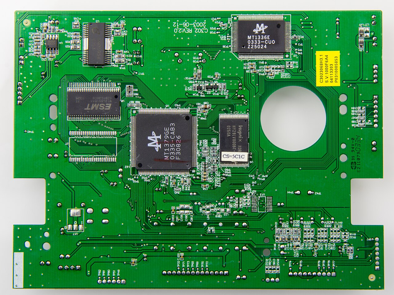](https://wiki.soonerrobotics.org/uploads/images/gallery/2026-10/f5pimage.png)
*https://en.wikipedia.org/wiki/Printed\_circuit\_board*
For more information on how PCB works, check out this video: [What are PCBs? || How do PCBs Work?](https://www.youtube.com/watch?v=Z2LgmIGE2nI)
## Altium Designer[](https://wiki.soonerrobotics.org/uploads/images/gallery/2026-10/mdLimage.png)
**Altium** is the premier industry-level PCB design software. Engineers primarily use Altium because it has a working unified design system, allowing you develop schematics, layouts, component libraries, manufacturing drawings, PCB CAD models, and much more in a single software.
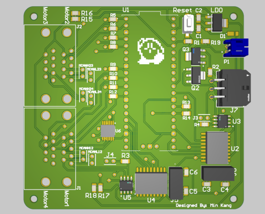
This makes Altium the ideal software for our robotics team. Below are examples of PCBs developed for our robots over the years:
[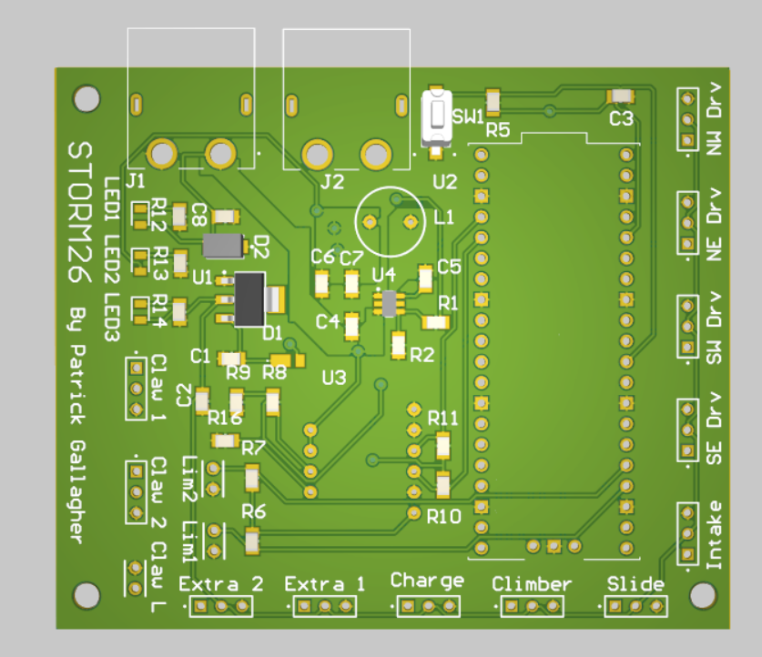](https://wiki.soonerrobotics.org/uploads/images/gallery/2026-10/v85image.png)
[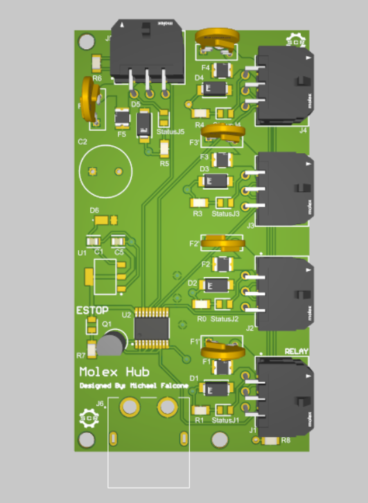](https://wiki.soonerrobotics.org/uploads/images/gallery/2026-10/IqUimage.png)
[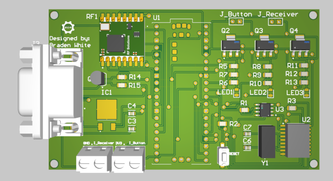](https://wiki.soonerrobotics.org/uploads/images/gallery/2026-10/VBkimage.png)
[](https://wiki.soonerrobotics.org/uploads/images/gallery/2026-10/hMuimage.png)
## Project Overview - SPI-CAN Breakout Board
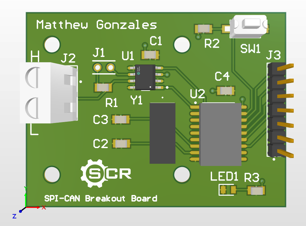
For this Altium tutorial, your goal is to recreate the PCB found below, **the SPI-CAN Breakout Board**.
[](https://wiki.soonerrobotics.org/uploads/images/gallery/2026-10/2ZCimage.png)
The SPI-CAN Breakout board provides a CAN (Controller Area Network) adapter to a microcontroller on another PCB. This is important since most microcontrollers communicate in SPI (Serial Peripherals Interface), but need to communicate with the robot and other boards in CAN. Just think of the board as a translater between the two communication protocols, SPI and CAN.
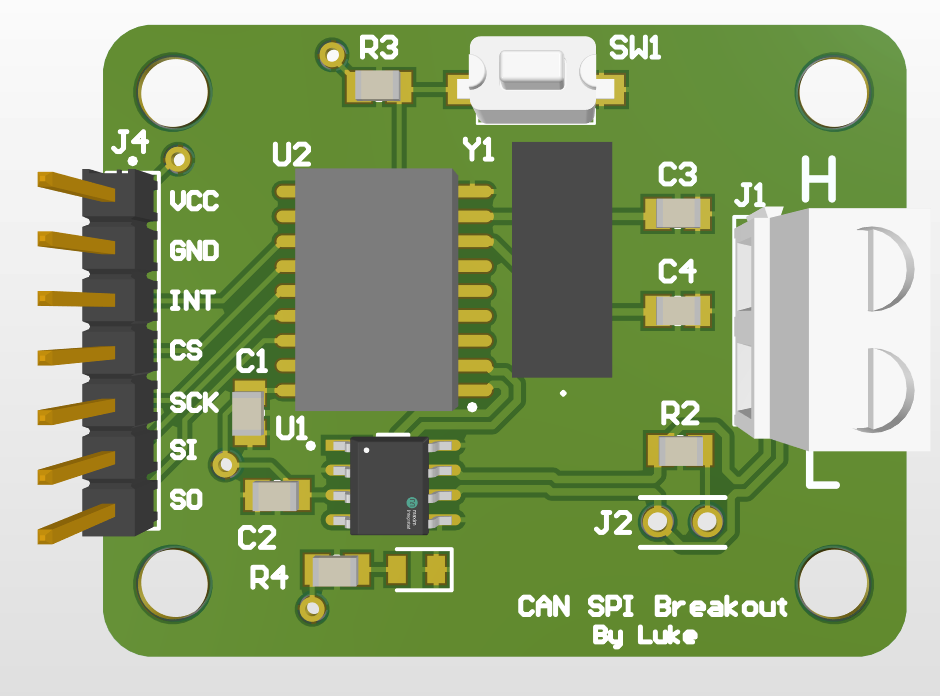
> *Note: This board is a revision of the the CAN-SPI Breakout Board from the 2026 IGVC Team, designed by Luke Finnegan.*
[](https://wiki.soonerrobotics.org/uploads/images/gallery/2026-10/PaYimage.png)
## Creating a Project
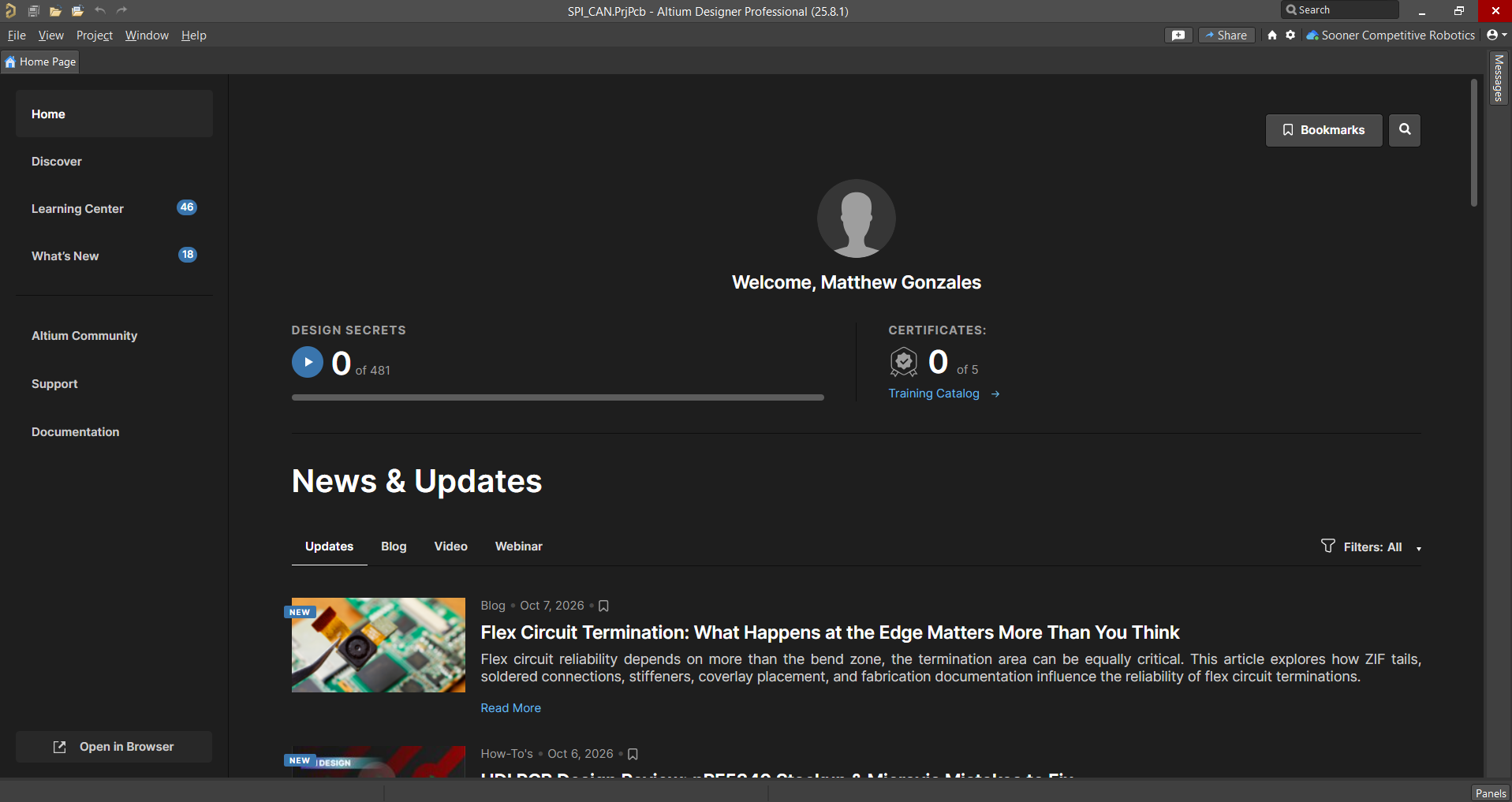
To start, open the Altium application on your device. Upon Altium loading, you should be greeted by a home page that looks similar to below:
[](https://wiki.soonerrobotics.org/uploads/images/gallery/2026-10/image.png)
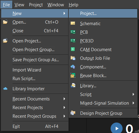
To start a new project, navigate to the top-left toolbar and select **File** --> select **New** --> then select **Project.**
[](https://wiki.soonerrobotics.org/uploads/images/gallery/2026-10/nZ3image.png)
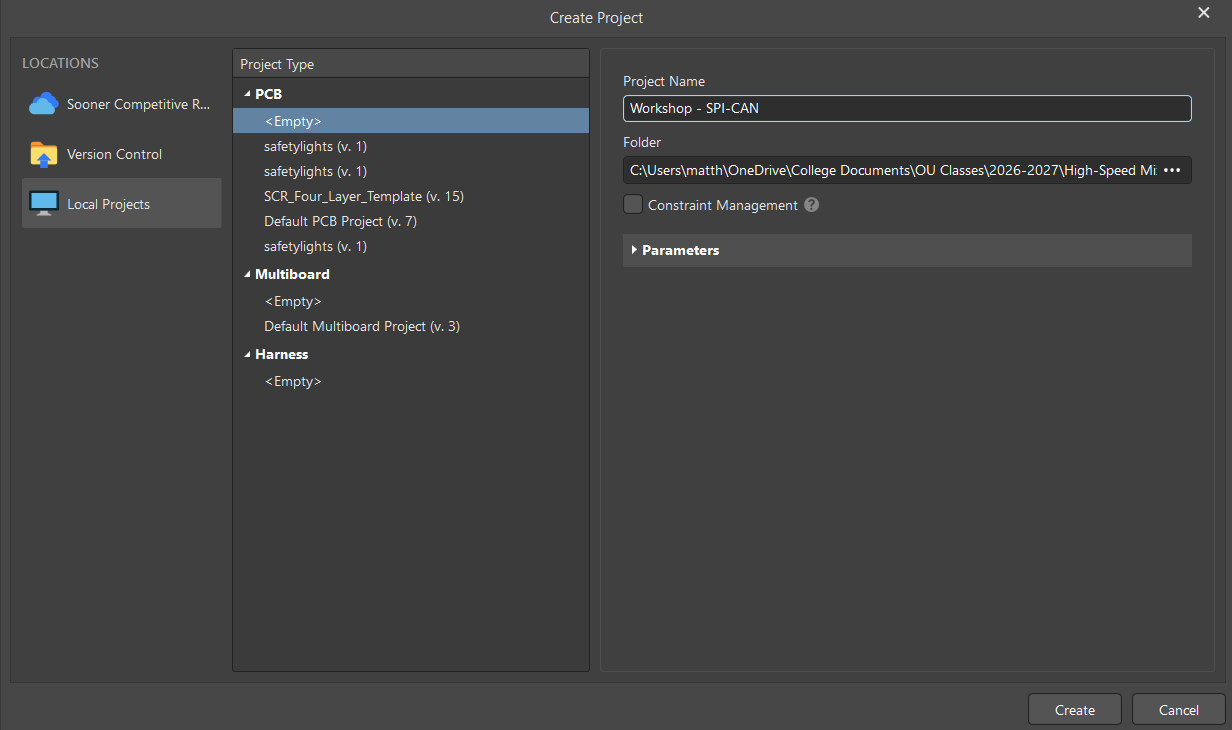
In the new window under **Project Name**, name your project "*Worshop - SPI-CAN*".
- Under **Folder**, make sure your project is saved in a file location you can find. You can change the file location by selecting the three dots "**...**" on the right.
[](https://wiki.soonerrobotics.org/uploads/images/gallery/2026-10/PrSimage.png)
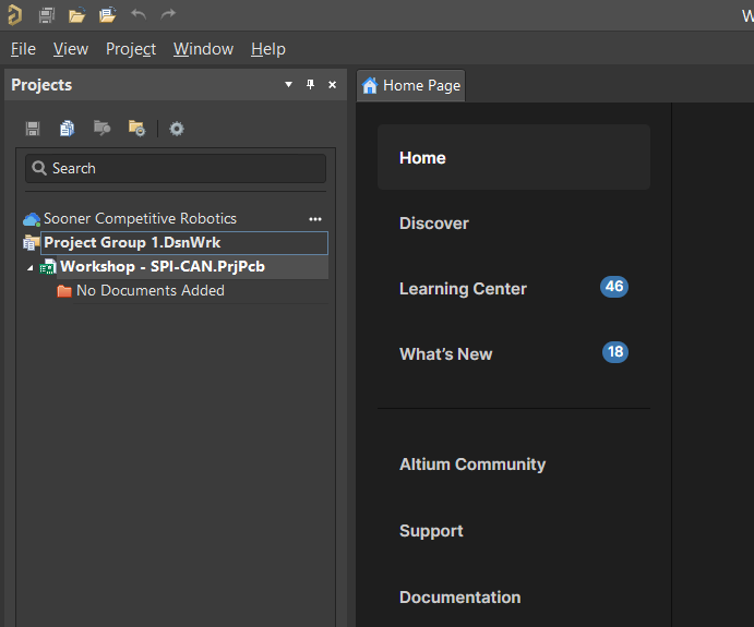
Upon creating a new project, the **Projects Panel** will now open, where you can view all your active projects. Your project's repository should be saved on your local device. For future designs, make sure to save it in the Sooner Competitive Robotics workspace.
[](https://wiki.soonerrobotics.org/uploads/images/gallery/2026-10/0kuimage.png)
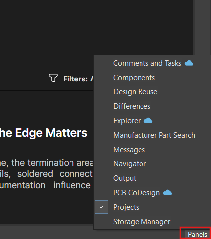
On the bottom right of your window, you'll find the **Panels** toggle. This toggle stores a ton of tools and will come in handy later. For now, just know you can reopen the Projects panel through accessing this toggle.
[](https://wiki.soonerrobotics.org/uploads/images/gallery/2026-10/ZlAimage.png)
## Adding to a Project
Now, your project is currently empty. To get started, you'll need to add documents by **right-clicking** on the "**Workshop - SPI-CAN.PrjPcb**" icon. In the new window, hover over **Add New to Project**, then you can add any documents you need.
[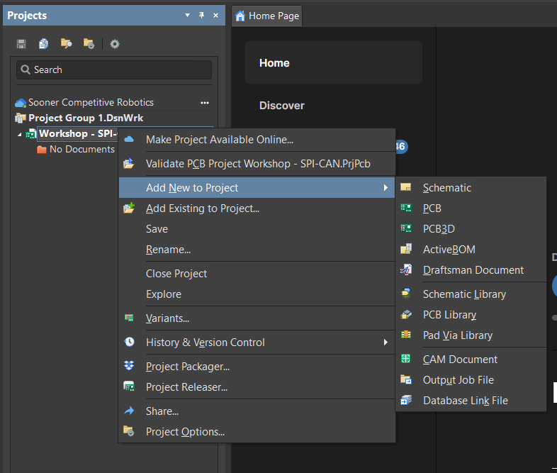](https://wiki.soonerrobotics.org/uploads/images/gallery/2026-10/4Dmimage.png)
Go ahead and add the following documents to your project:
- Schematic
- PCB
- ActiveBOM
- Draftsman Document
- Assembly Drawing
- Fabrication Drawing
- Output Job File
For the Draftsman Documents, a new window will appear. For the Assembly Drawing, select **Assembly Drawing ANSI-B (v. 3),** then press **OK**. For the Fabrication Drawing, select **Fabrication Drawing ANSI-B (v. 3),** then press **OK**.
[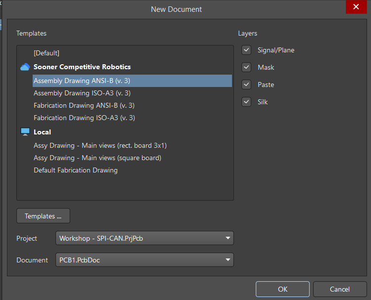](https://wiki.soonerrobotics.org/uploads/images/gallery/2026-10/v4bimage.png)
After you add the required documents to your project, your Projects panel should look like the screenshot below:
[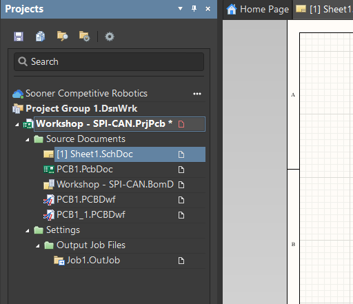](https://wiki.soonerrobotics.org/uploads/images/gallery/2026-10/57himage.png)
Before you start your design, you'll need to save each of your documents and rename them accordingly. To save a document, right-click on the document's icon, then select **Save.**
[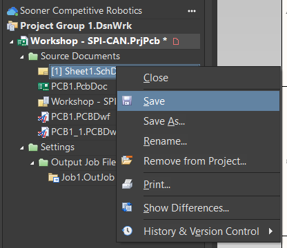](https://wiki.soonerrobotics.org/uploads/images/gallery/2026-10/JaSimage.png)
Rename each of the documents until they match the names below:
[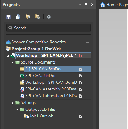](https://wiki.soonerrobotics.org/uploads/images/gallery/2026-10/ozvimage.png)
Congratulations! You just finished creating your first Project! Now, you can get started on the schematic by accessing the tutorial: [2. Creating a Schematic](https://wiki.soonerrobotics.org/books/pcb-design-altium-how-to/page/2-creating-a-schematic)
# 2. Creating a Schematic
## Introduction
Creating a schematic in Altium is one of the most important steps in PCB Design. Before you create a schematic from scratch, you should already have a good idea about what your PCB will be used for, the logic behind the design, and critical components that will allow for successful operation.
**During the schematic design process, you'll typically follow these steps:**
1. Requirements - Deciding the necessary interfaces, constraints, etc.
2. Project Libraries - Determining which components are needed for your design.
3. Component Arrangement - Organizing and wiring the components on your sheet.
4. ERC / Compiling - Checking for errors and validating your schematic
> *Note: It's **HIGHLY** recommended to use a computer mouse when going through this tutorial.*
## Schematic Sheet Set-Up
When you start, you should already have a blank schematic loaded.
- For information on how to create a blank schematic, refer to [1. Project Creation](https://wiki.soonerrobotics.org/books/pcb-design-altium-how-to/page/1-project-creation)
[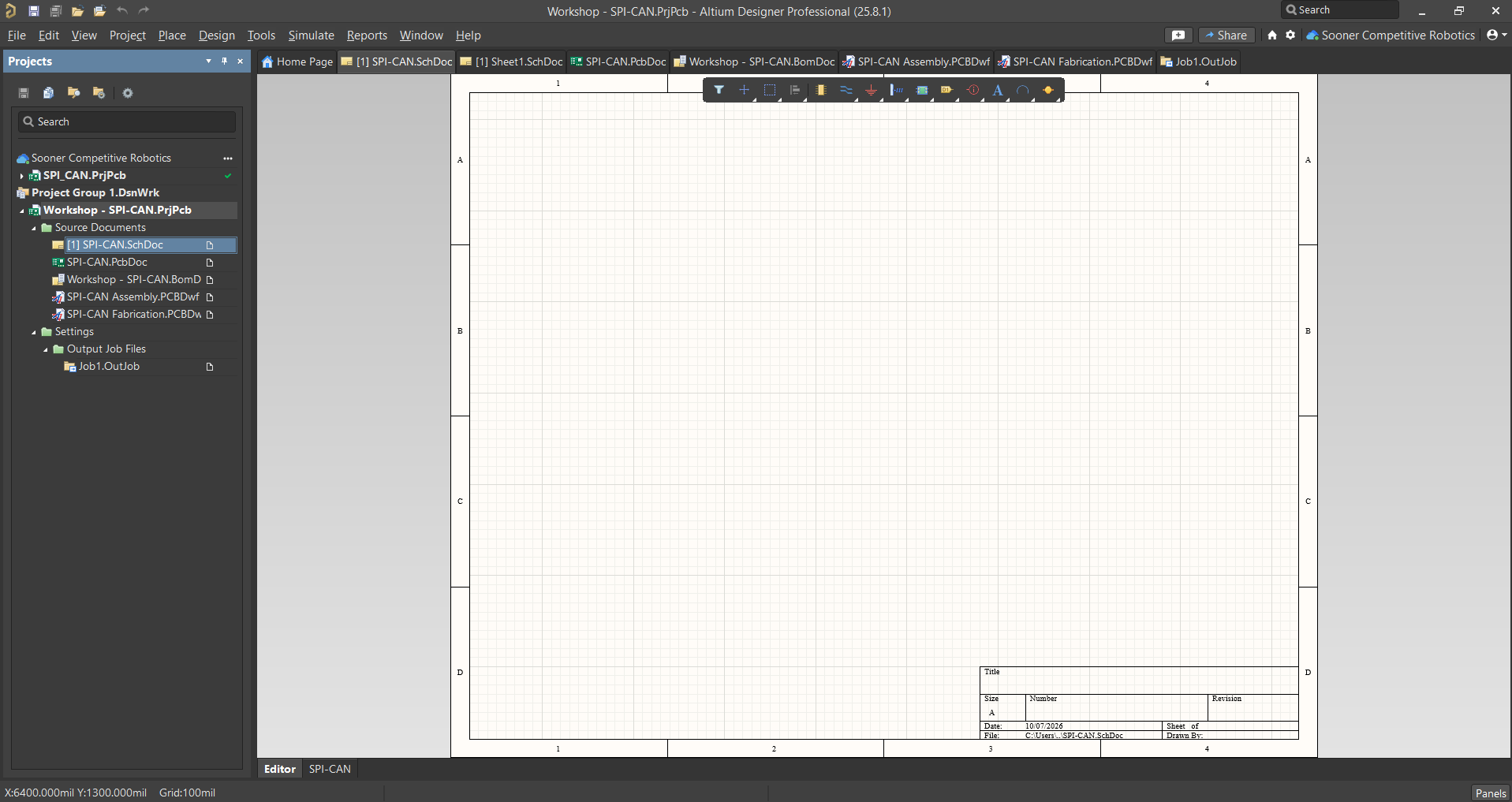](https://wiki.soonerrobotics.org/uploads/images/gallery/2026-10/I1dimage.png)
> *As you're creating your schematic, it's helpful to know these controls:*
>
> - *Right-Click & Hold: Moves the Page*
> - *Scroll Wheel: Move up and down on the Page*
> - *Ctrl + Scoll Wheel: Zooms in-and-out of the Page*
Before designing your circuit schematic, it's important to make sure your sheet has everything set-up properly. This includes the Sheet size, title, author, and more.
To start, navigate to the bottom-right of the window and select **Panels** --> then select **Properties**
[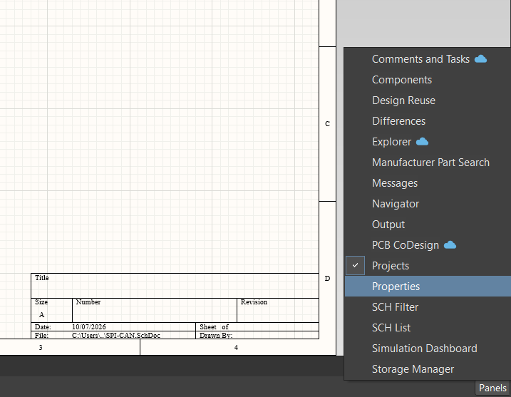](https://wiki.soonerrobotics.org/uploads/images/gallery/2026-10/g6Dimage.png)
A new window should appear as seen below:
[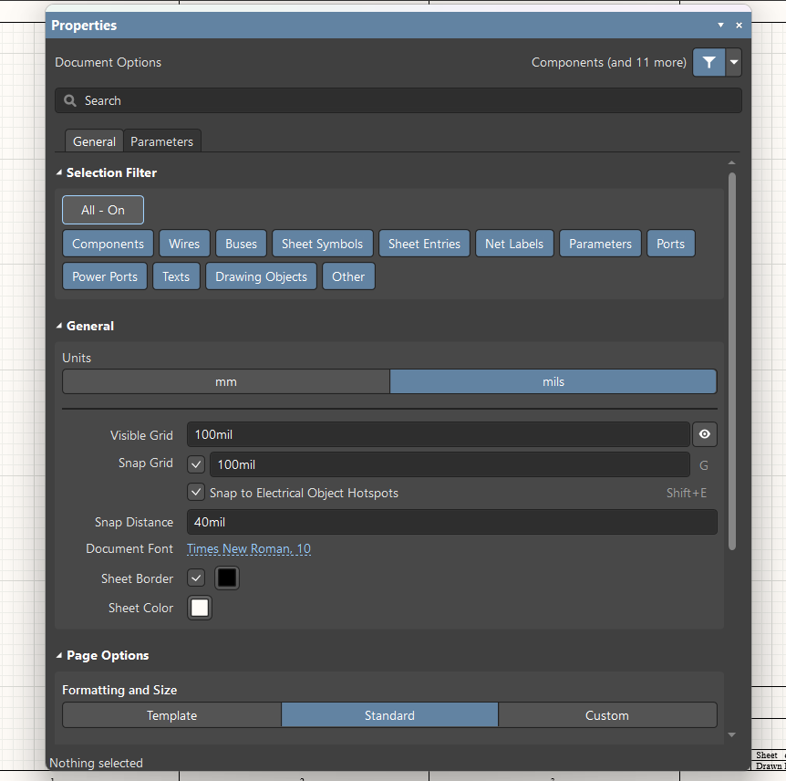](https://wiki.soonerrobotics.org/uploads/images/gallery/2026-10/apCimage.png)
If you scroll down, you can modify the Sheet Size, Orientation, and more! For now, we'll leave the settings as they are.
[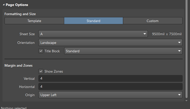](https://wiki.soonerrobotics.org/uploads/images/gallery/2026-10/ES5image.png)
If you select the Parameters tab (under the Search Bar), you can modify the sheet's elements.
[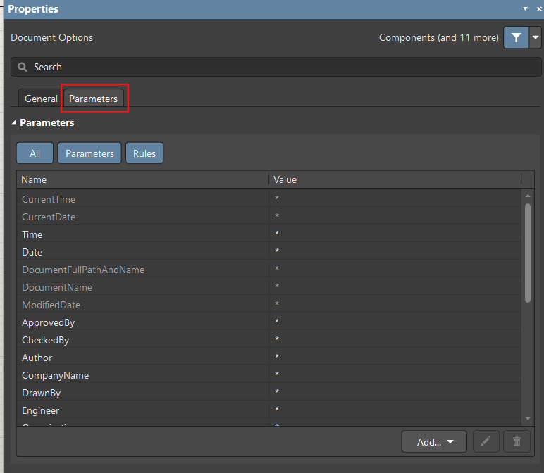](https://wiki.soonerrobotics.org/uploads/images/gallery/2026-10/Tvuimage.png)
Go ahead and modify the following parameters with the following values:
- Date - **Today's Date**
- Author - **Your Name**
- Title - **"SPI-CAN Breakout Board"**
- DocumentNumber - **1**
- Revision - **1**
Next, you'll need to place these values on the sheet. With the values set, exit out of the properties window and navigate to the top of the window.
You'll find a tool-bar filled with various icons. Hover over the "**A**" icon and right-click until a drop-down appears. Then, select **Text String**.
[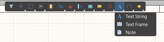](https://wiki.soonerrobotics.org/uploads/images/gallery/2026-10/ltrimage.png)
You'll see the word "Text" appear and move along with your cursor. To place it on your schematic, simply left-click on the sheet.
[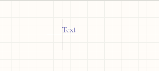](https://wiki.soonerrobotics.org/uploads/images/gallery/2026-10/rwhimage.png)
Like all objects placed on a schematic, you can **left-click and hold down** on an object to move it around. With this in mind, place a bunch of text boxes in the title block as arranged below:
[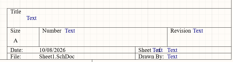](https://wiki.soonerrobotics.org/uploads/images/gallery/2026-10/9P8image.png)
To update the text, right-click on a Text box, then select **Properties**
[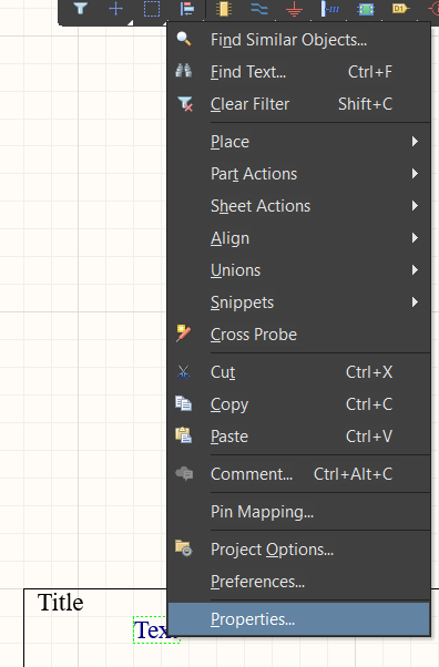](https://wiki.soonerrobotics.org/uploads/images/gallery/2026-10/xxJimage.png)
Next, in the drop-down arrow in the **Text** box, navigate to the value you want to attribute to your text box.
[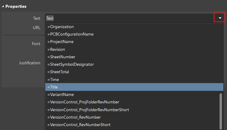](https://wiki.soonerrobotics.org/uploads/images/gallery/2026-10/NbZimage.png)
Go ahead and update the text boxes using the procedure above. You can also update the text size and color to your liking.
[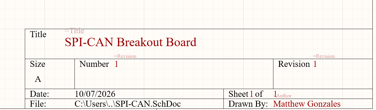](https://wiki.soonerrobotics.org/uploads/images/gallery/2026-10/mi2image.png)
## Component Selection & Placement:
You're now ready to begin placing components on your board. Typically, you'll need to conduct proper research on your circuit design beforehand. Fortunately, we have a design ready for you!
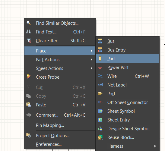
Start by right-clicking anywhere on the schematic. Then, select **Place** --> select **Part.**
[](https://wiki.soonerrobotics.org/uploads/images/gallery/2026-10/fSgimage.png)
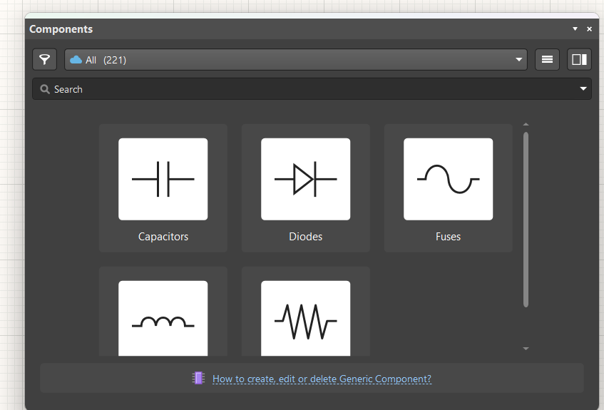
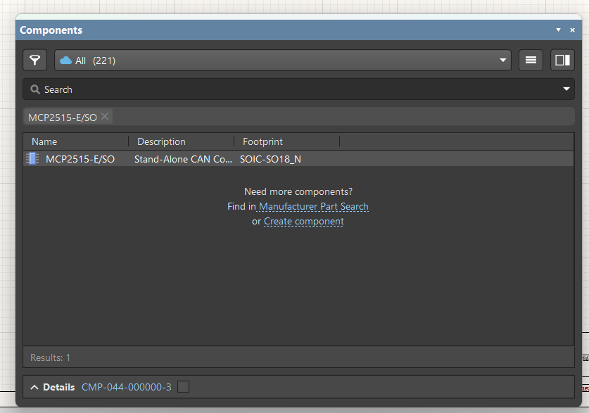
A new window should appear, allowing you to search for parts from the Sooner Competitive Robotics workspace components library. To start, go ahead and insert the text "**MCP2515-E/SO**" into the Search box.
[](https://wiki.soonerrobotics.org/uploads/images/gallery/2026-10/YuGimage.png)
You should see the part you searched up appear below. If your desired component is not saved to SCR's custom parts library, you can always search for parts in the **Manufacturer Part Search**.
[](https://wiki.soonerrobotics.org/uploads/images/gallery/2026-10/SXZimage.png)
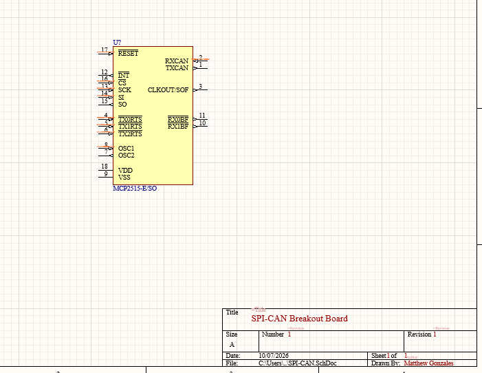
To place your part, double left-click the part's icon. A faded version of your part should appear on your schematic. Left-click on the sheet to place your part. Press **esc** on your keyboard to exit out of part placement.
Once you exit out of the Components window, your part should appear on the page like below:
[](https://wiki.soonerrobotics.org/uploads/images/gallery/2026-10/fFPimage.png)
For one of the components, we'll need to access the Manufacturer Part Search. Open the Components window, then search up the part number "**TSW-107-07-G-S.**" You'll notice this part doesn't appear in the search results since it's not stored in the SCR components library.
[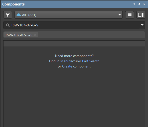](https://wiki.soonerrobotics.org/uploads/images/gallery/2026-10/86Cimage.png)
Go ahead and navigate to the Manufacturer Part Search. The part you searched for should now appear.
[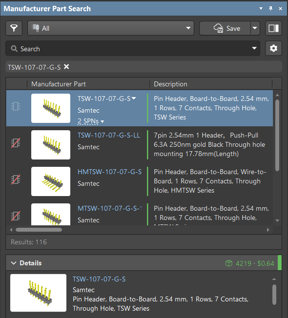](https://wiki.soonerrobotics.org/uploads/images/gallery/2026-10/4k2image.png)
You can expand the **SPNs** tab. This will display the vendors that are currently selling the component.
[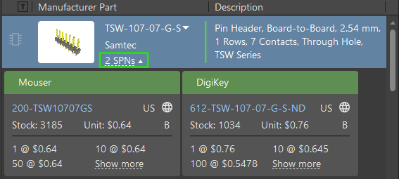](https://wiki.soonerrobotics.org/uploads/images/gallery/2026-10/t04image.png)
We'll go ahead and place the component from the top search result. To do so, right-click on the **TSW-107-07-G-S**, then select **Place**.
[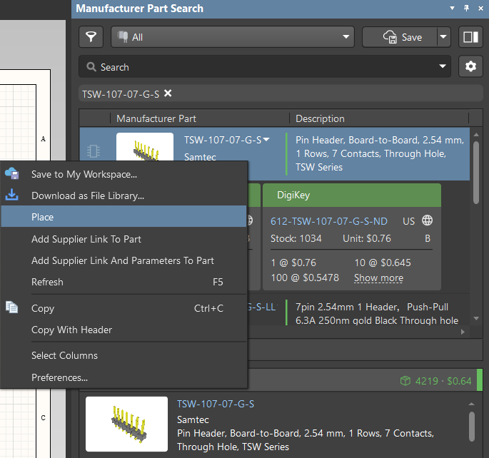](https://wiki.soonerrobotics.org/uploads/images/gallery/2026-10/Zz6image.png)
Place down your part. Your schematic should look like below.
[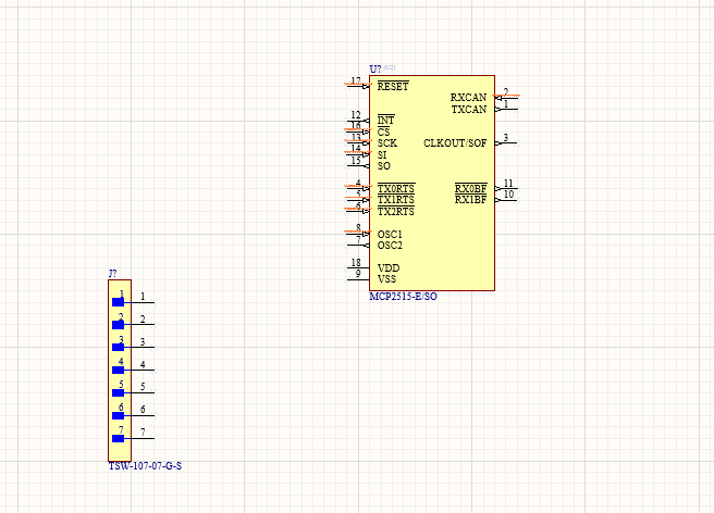](https://wiki.soonerrobotics.org/uploads/images/gallery/2026-10/rhKimage.png)
Now, go ahead and place the required parts for your project using the procedure you just learned. A list of the required parts can be found below:
> *Note: for the capacitors and resistors, you're going to search up the string in bold. After placing the component, you'll modify the part's properties with it's required values. Info on how to do this is after the component list.*
- 1x MCP2515-E/SO
- 1x MAX3051ESA+
- 1x LFXTAL057135Bulk
- 1x 2x1 Header
- 1x TSW-107-07-G-S
- 1x 2x1 screw terminal
- 1x AP2012SGD3
- 1x 6mmx3.5mm SMD Switch
- **GENERIC CAPACITOR 0805 or 0603(1608):**
- 2x 18pF
- 2x 0.1uF
- **0805 RES:**
- 1x 120Ω
- 1x 220Ω
- 1x 10KΩ
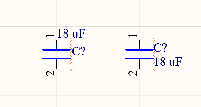
Whenever you place down a capacitor, resistor, or any component with a custom value, you'll need to showcase the value on the schematic. When you place a capacitor, you'll see something like this:
[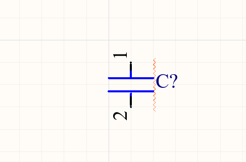](https://wiki.soonerrobotics.org/uploads/images/gallery/2026-10/px2image.png)
To assign the capacitor's value, double left-click on the newly placed component. Next, type in the capacitor's value into the Comment text box. Afterward, make sure the "eye" icon is enabled before closing out of your window.
[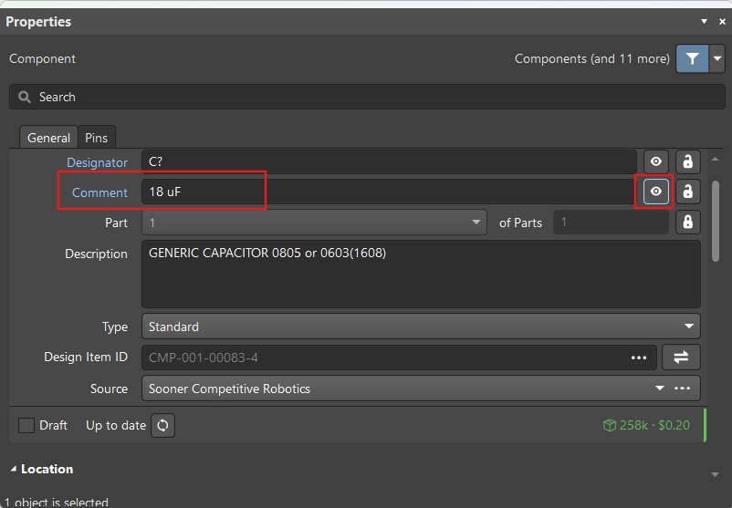](https://wiki.soonerrobotics.org/uploads/images/gallery/2026-10/8YJimage.png)
Then, scroll down to parameters and disable the eye icon for the **Values** parameter.
[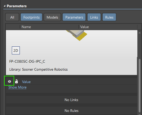](https://wiki.soonerrobotics.org/uploads/images/gallery/2026-10/nycimage.png)
Your component should look like the capacitor on the left. You can move around the text surrounding the capacitor to make it more organized.
[](https://wiki.soonerrobotics.org/uploads/images/gallery/2026-10/4ukimage.png)
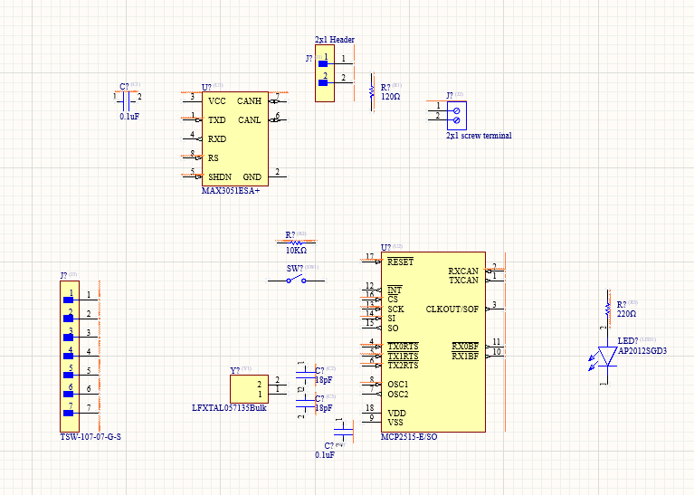
You can follow the same process for your resistors. When you're finished placing components, your schematic should look like the following:
[](https://wiki.soonerrobotics.org/uploads/images/gallery/2026-10/w9Vimage.png)
## Power Ports:
Next, you'll to place your Power and Ground references. These are necessary to understand how power flows through your circuit.
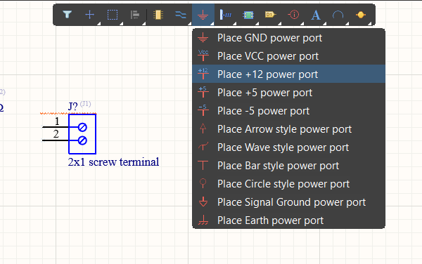
To start, navigate to the top tool-bar and right-click on the ground symbol (the upside down tree). You'll see multiple power references to select from. For our purposes, selected the **Place +12 power port**.
[](https://wiki.soonerrobotics.org/uploads/images/gallery/2026-10/NEJimage.png)
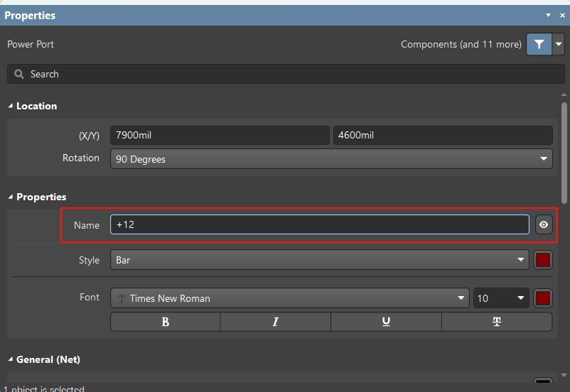
Once you place your power port, you'll need to update the value to **+3.3 V**. Double-click on the port you just placed and change the name from **+12** to **3.3V**.
[](https://wiki.soonerrobotics.org/uploads/images/gallery/2026-10/Kjgimage.png)
Now, go ahead and place a GND port. When you're done, you should have two ports placed as seen below:
[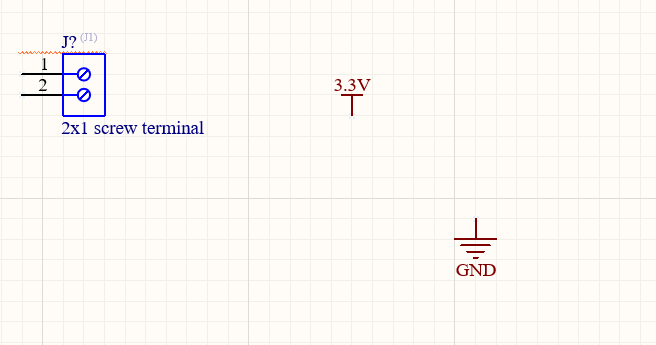](https://wiki.soonerrobotics.org/uploads/images/gallery/2026-10/gMPimage.png)
Go ahead and arrange the ports to their appropriate locations as seen below. Copy and Paste each port until you have:
- 10x GND Ports
- 5x 3.3V Ports
> *Note: While placing a component, you can press Space to rotate your part 90 degrees!*
[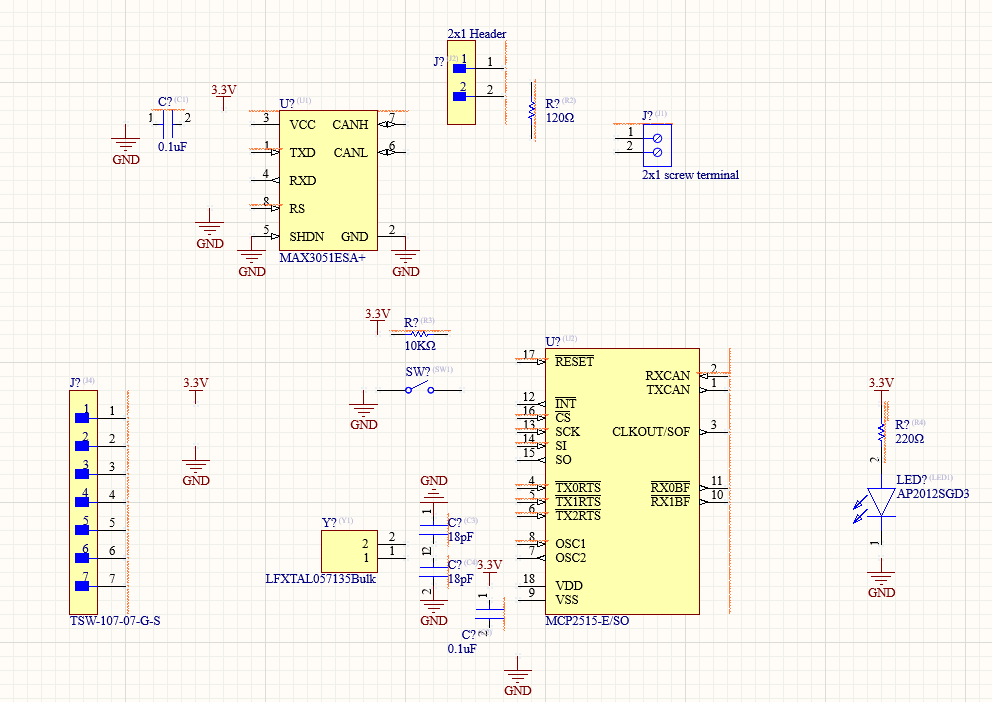](https://wiki.soonerrobotics.org/uploads/images/gallery/2026-10/L08image.png)
## Component Wiring:
With your components laid out, we can go ahead and mark off any ports we're not using for our design.
To do this, navigate to the top tool-bar and right-click on the **Place Parameter Set** icon (the circled "i"). Then, select the **Generic No ERC** item.
[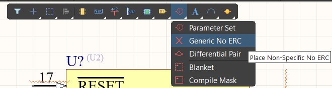](https://wiki.soonerrobotics.org/uploads/images/gallery/2026-10/8nfimage.png)
Then, go ahead and mark the following pins on the **MCP2515-E/SO** with the no connection indicator:
- TX0RTS
- TX1TS
- TX2RTS
- CLKOUT/SOF
- RX0BF
- RX1BF
[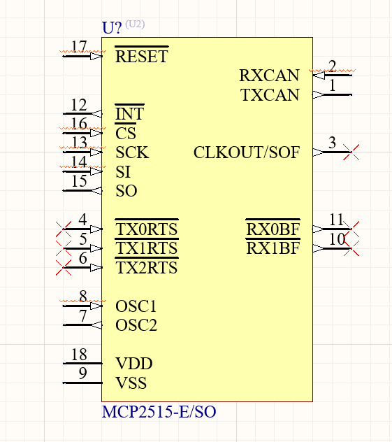](https://wiki.soonerrobotics.org/uploads/images/gallery/2026-10/h33image.png)
Now, you can start **wiring** your components together. To enable the wire toggle, there's a couple of ways to do this.
First, you can navigate to the top toolbar and right-click on the wire icon (the two blue wavy lines). In the drop-down box, select **Wire.**
- You can do the same thing by selecting **Ctrl + W** on your keyboard.
[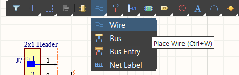](https://wiki.soonerrobotics.org/uploads/images/gallery/2026-10/mOJimage.png)
On your sheet, you should now see a faded cross-hair moving with your cursor. Wherever you left-click on the sheet, a wire will form.
Let's connect the 3.3V power port to the 2x1 Header. With the wire toggle enabled, left-click on the "1" port and drag your invisible wire to the 3.3V port. Left-click on the 3.3V port to connect your wire.
[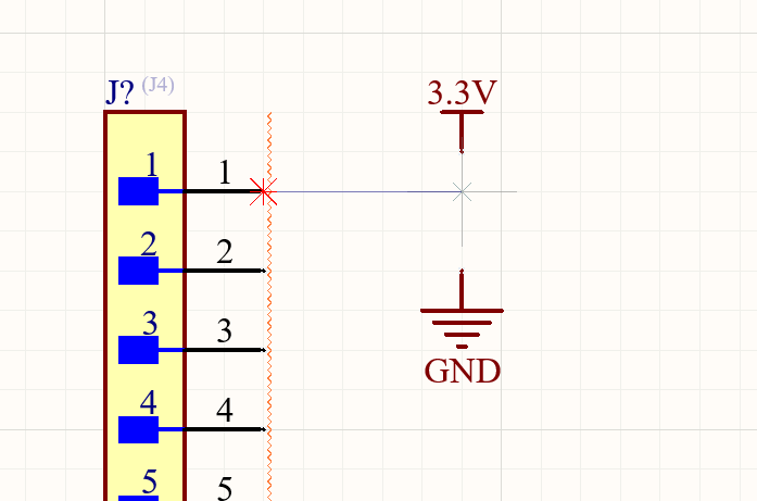](https://wiki.soonerrobotics.org/uploads/images/gallery/2026-10/wN3image.png)[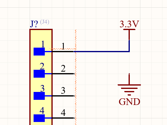](https://wiki.soonerrobotics.org/uploads/images/gallery/2026-10/Lhximage.png)
> *Note, for any components or wires on the sheet, you can remove them by selecting those objects and pressing **delete** on your keyboard.*
In addition to wiring, you can place **Net Labels** on your schematic to connect two ports. Net labels are basically just wires, but without the physical traces going across the sheet.
To select a Net Label, navigate to the top tool-bar and select the wire icon. In the drop-down box, select **Net Label**.
[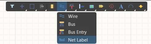](https://wiki.soonerrobotics.org/uploads/images/gallery/2026-10/mcKimage.png)
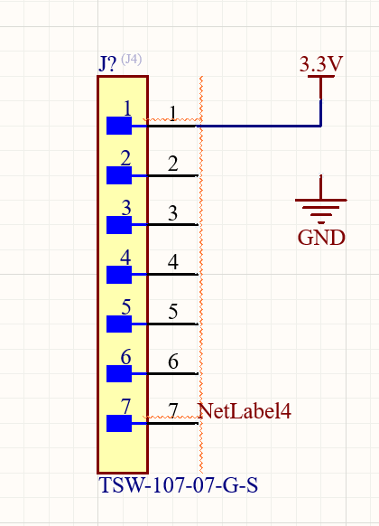
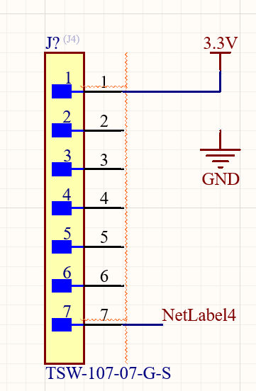
Attach the Net Label to port 7 on the 2x1 Header. You can left-click and drag the net label away from the port. When you do this, a wire will show, indicating the net label and port are connected.
[](https://wiki.soonerrobotics.org/uploads/images/gallery/2026-10/YSyimage.png)
[](https://wiki.soonerrobotics.org/uploads/images/gallery/2026-10/gwBimage.png)
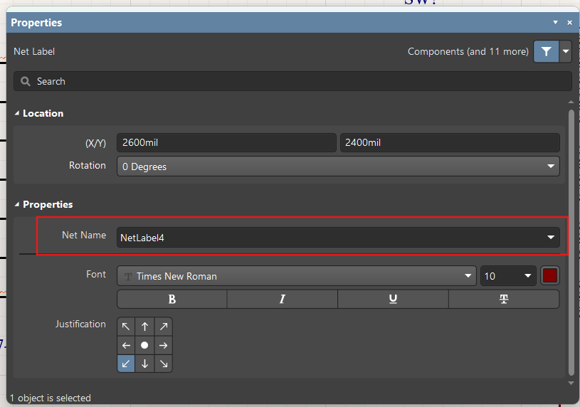
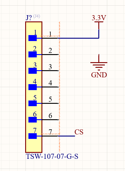
Now, double left-click on the newly placed Net Label, and rename it to "**CS**".
[](https://wiki.soonerrobotics.org/uploads/images/gallery/2026-10/c6Vimage.png)
You should now have something similar to below:
[](https://wiki.soonerrobotics.org/uploads/images/gallery/2026-10/Necimage.png)
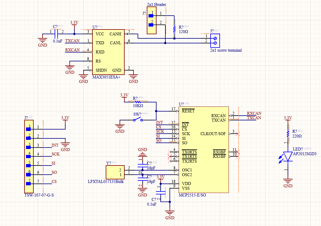
Using the tools you just learned, connect the components with wires and Net labels as seen below:
> *Note: when you complete your wiring, double-check your design to make sure everything is wired up correctly.*
[](https://wiki.soonerrobotics.org/uploads/images/gallery/2026-10/fKIimage.png)
## Schematic Annotation:
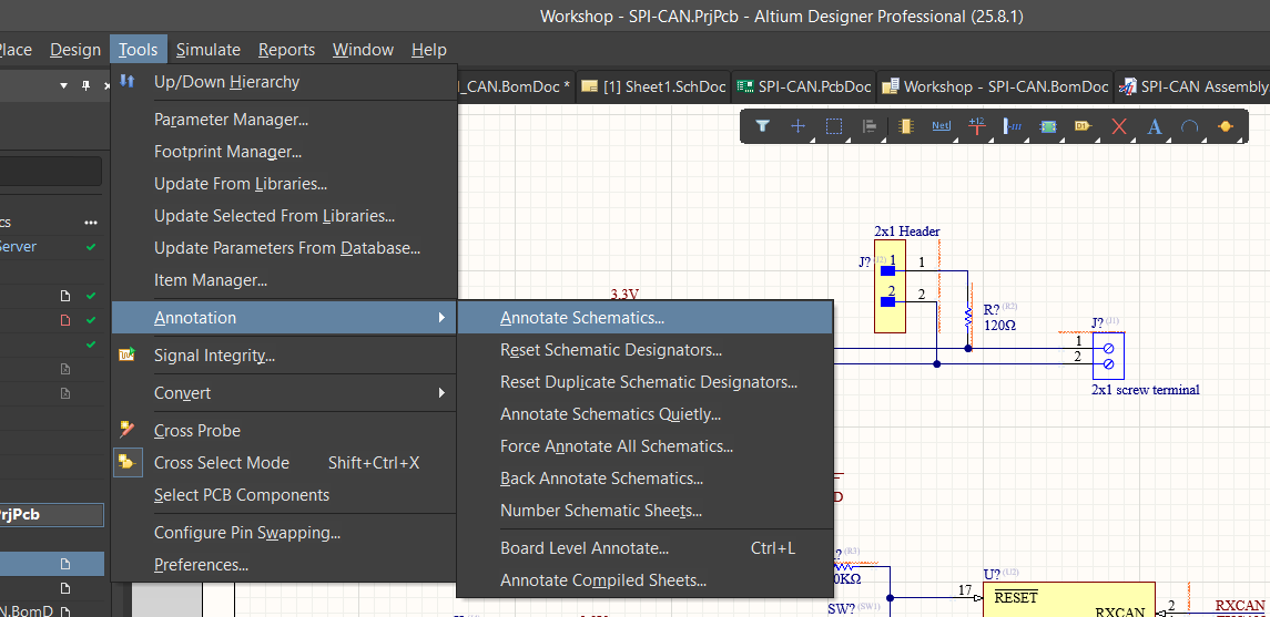
Once everything is wired up correctly, you're now ready to annotate your schematic. To do this, navigate to the top left tool-bar and select **Tools** --> select **Annotation** --> then select **Annotate Schematics**.
[](https://wiki.soonerrobotics.org/uploads/images/gallery/2026-10/oUgimage.png)
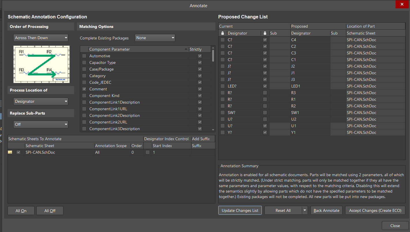
A new window should appear. You can modify how the annotation is laid out on the schematic.
[](https://wiki.soonerrobotics.org/uploads/images/gallery/2026-10/XYZimage.png)
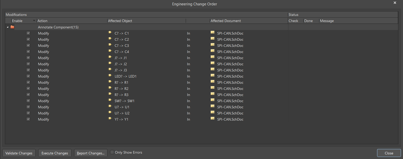
Once you're satisfied with the settings, select **Update Changes List -->** select **OK** --> then select **Accept Changes (Create ECO)**. A new window should appear:
[](https://wiki.soonerrobotics.org/uploads/images/gallery/2026-10/C4Eimage.png)
To finalize the modifications, select **Validate Changes** --> then select **Execute Changes**. Once the green checkmarks appear under each part's status, close out of both windows. Your schematic should now look like what's seen below:
[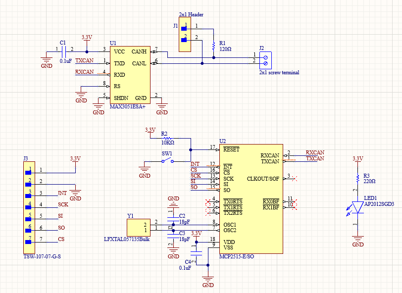](https://wiki.soonerrobotics.org/uploads/images/gallery/2026-10/cQLimage.png)
Now that your schematic is finished, you're ready to validate the design. Navigate to the Projects panel on the left side, right-click on the **Workshop - SPI-CAN.Prj.Pcb** icon, then select **Validate PCB Project** **Workshop - SPI-CAN.Prj.Pcb.**
[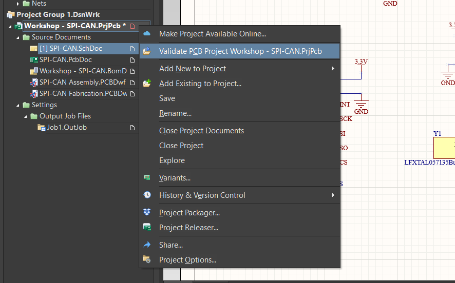](https://wiki.soonerrobotics.org/uploads/images/gallery/2026-10/3s2image.png)
To chech the results of the validation, navigate to the Panels toggle and select **Messages.**
[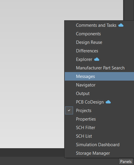](https://wiki.soonerrobotics.org/uploads/images/gallery/2026-10/7Nrimage.png)
A new window should appear on the right side of your screen.
[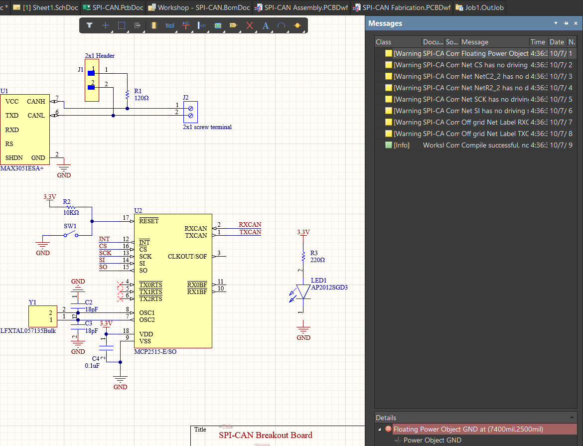](https://wiki.soonerrobotics.org/uploads/images/gallery/2026-10/qILimage.png)
From the Electric Rule Check (ERC) validation, we received a bunch of warnings and an info block that tells us our design works. This is good! If you end up with messages that are proceeded with an orange box labeled **Error**, then you have some critical issues with your design that need to be fixed.
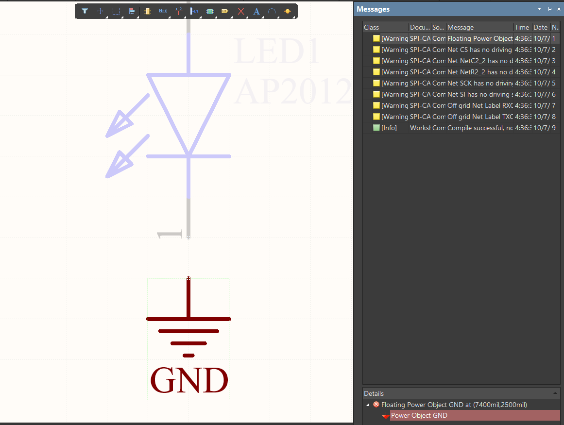
To tell exactly where an warning / error lives on your schematic, simply double left-click on the message. For instance, by investigating the message **Floating Power Object**, we see that there's a missing connection between LED1 and it's GND reference.
- We left this disconnected on purpose to see this appear in the validation check. Go ahead and insert the connection, then run the validation check again.
[](https://wiki.soonerrobotics.org/uploads/images/gallery/2026-10/rO0image.png)
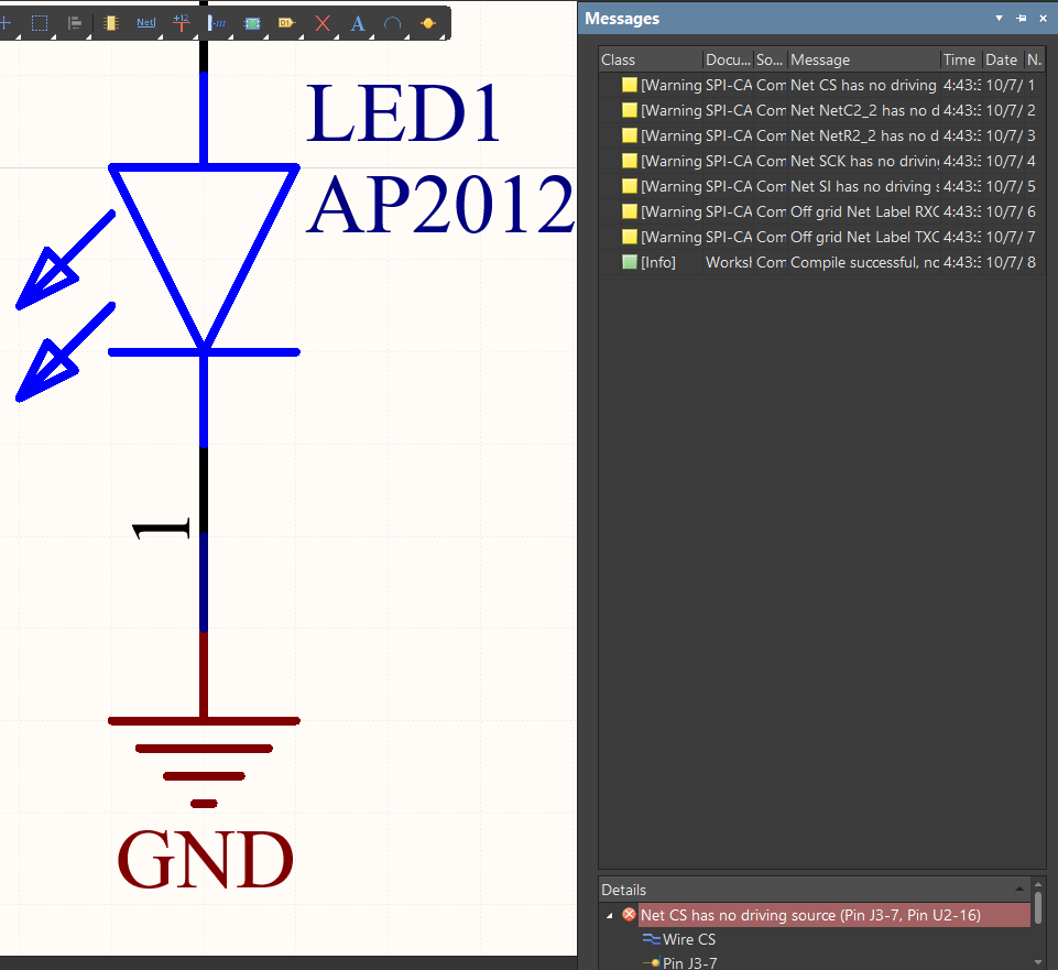
Upon opening Messages again, you'll see that the warning has dissapeared.
[](https://wiki.soonerrobotics.org/uploads/images/gallery/2026-10/4d6image.png)
Now, we don't have to worry about the rest of these warnings for this design. Ideally, your designs should have no warnings or errors after validation.
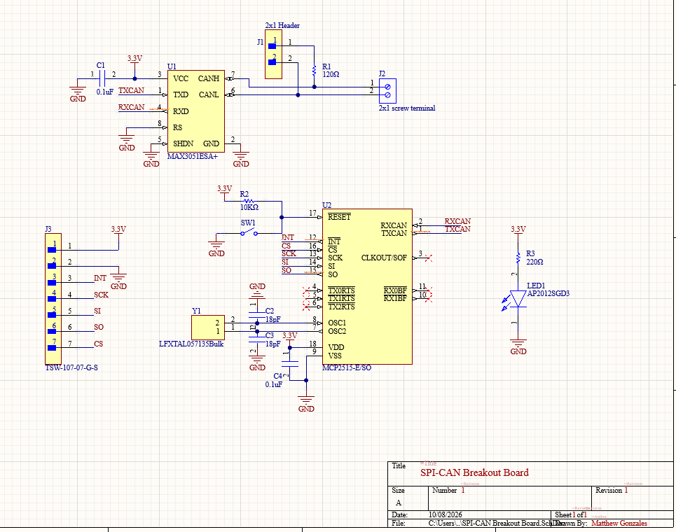
**Congratulations**! You just created your first PCB schematic! At this stage, you'd typically allow our lovely SCR mentors and alumni to review your design and provide feedback for revisions. Fortunately, this design has alreayd been reviewed.
[](https://wiki.soonerrobotics.org/uploads/images/gallery/2026-10/sLFimage.png)
To learn about how to conduct a PCB layout, head to the next part of this tutorial: [3. Board Layout Pt. I](https://wiki.soonerrobotics.org/books/pcb-design-altium-how-to/page/3-board-layout-pt-i)
# 3. Board Layout Pt. I
## Introduction
After you complete a schematic, the next step in the PCB design process is to conduct the layout for your board. In doing so, you're translating the theoretical arrangement of your circuit design onto a physical board that will have to operate in the real world.
**During the layout process, you'll typically follow the steps below:**
1. Board & Stackup: Outlining layers and arranging the via stack-up.
2. Design Rules: Configuring the constraints of the layout to your design requirements.
3. Component Placement: Arranging components on the board and maximizing functionality.
4. Routing: Connecting components together, sometimes between multiple layers.
5. Design Rule Check (DRC): Verifying that your layout confines to the requirements outlined in the Design Rules.
> *Remember, there are many solutions for a design's board layout. It's your job to determine the best viable solution!*
## Layout Set-Up
Before you begin, keep in mind this tutorial is a continuation of the previous module's schematic.
- If you haven't already, please create the appropriate schematic by referring to [2. Creating a Schematic](https://wiki.soonerrobotics.org/books/pcb-design-altium-how-to/page/2-creating-a-schematic)
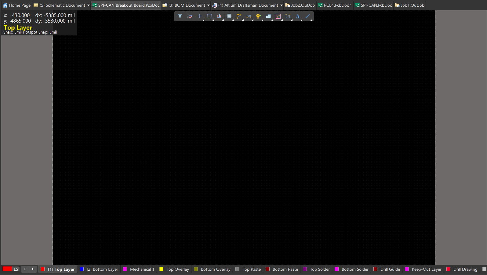
To start, open the PCB document for the SPI-CAN Breakout Board project you created earlier. You should have a window similar to below:
[](https://wiki.soonerrobotics.org/uploads/images/gallery/2026-10/al6image.png)
If you zoom out of the page slightly, you'll notice an odd cross-hair on the bottom left of the window. This is the **Origin**, the reference point for your layout's dimensions. When placing down components at specific measurements, it's nice to have the origin level with your board.
To place the origin in the correct spot, navigate to the top-left tool bar. Then, select **Edit** --> select **Origin** --> then select **Set**.
[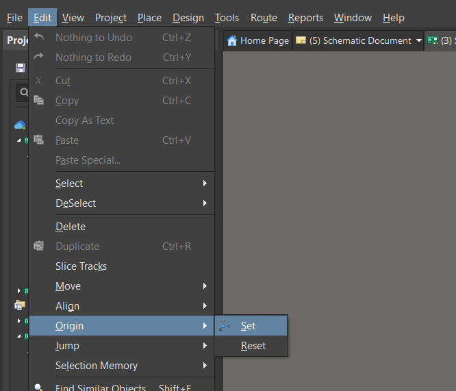](https://wiki.soonerrobotics.org/uploads/images/gallery/2026-10/x13image.png)
Now, a green cross should appear with your cursor. Place the green cross on the bottom left corner of your board border. Once your cursor is at the desired spot, use left-click to set the origin.
> *Note: You can use **Ctrl + Mouse Scroll Wheel** to zoom in on the corner!*
[](https://wiki.soonerrobotics.org/uploads/images/gallery/2026-10/M6ximage.png)
After zooming out, your layout should now look like what's seen below:
[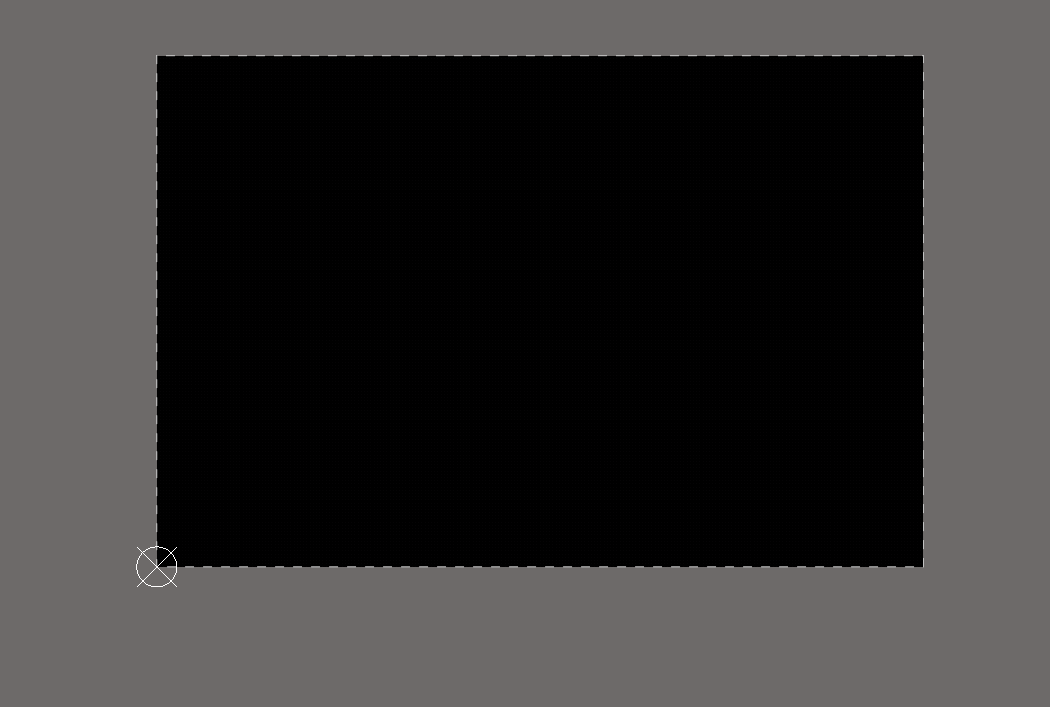](https://wiki.soonerrobotics.org/uploads/images/gallery/2026-10/kdRimage.png)
Now, since we only have about 15 components, we want to make our board smaller to save space and reduce manufacturing costs. To do this, we need to redefine the board shape.
In the top left tool-bar select **View** --> then select **Board Planning Mode.**
[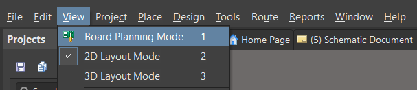](https://wiki.soonerrobotics.org/uploads/images/gallery/2026-10/QVhimage.png)
Your layout should now be in Board Planning mode, so your screen should look like this:
[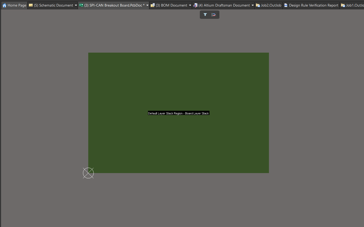](https://wiki.soonerrobotics.org/uploads/images/gallery/2026-10/7drimage.png)
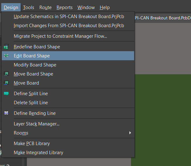
In the top left tool-bar, navigate to **Design** --> then select **Edit Board Shape.**
[](https://wiki.soonerrobotics.org/uploads/images/gallery/2026-10/LY5image.png)
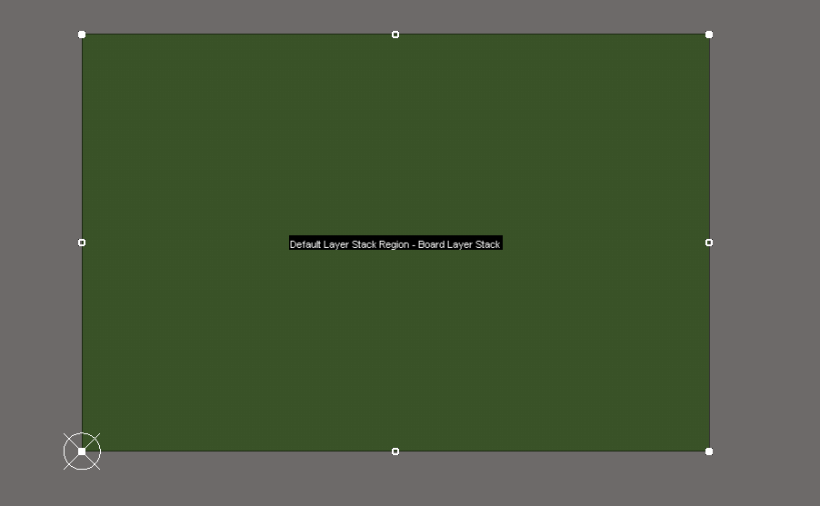
A white outline should appear around your board shape.
[](https://wiki.soonerrobotics.org/uploads/images/gallery/2026-10/EKdimage.png)
You'll want to change the board shape such that you have the following parameters:
- Length = 2000 mils
- Width = 1500 mils
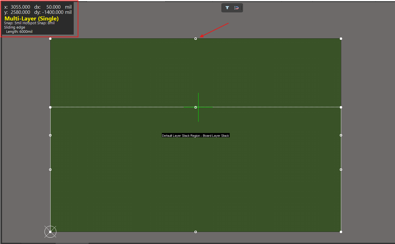
To change the board lengths, pick a side (top or right, move toward the origin) and select the center of the edge. Then, click and drag the edge until your board is the correct size.
- Use the legend on the top left to determine when your side is the correct size. Remember, you can zoom in to get a more precise placement.
[](https://wiki.soonerrobotics.org/uploads/images/gallery/2026-10/HVCimage.png)
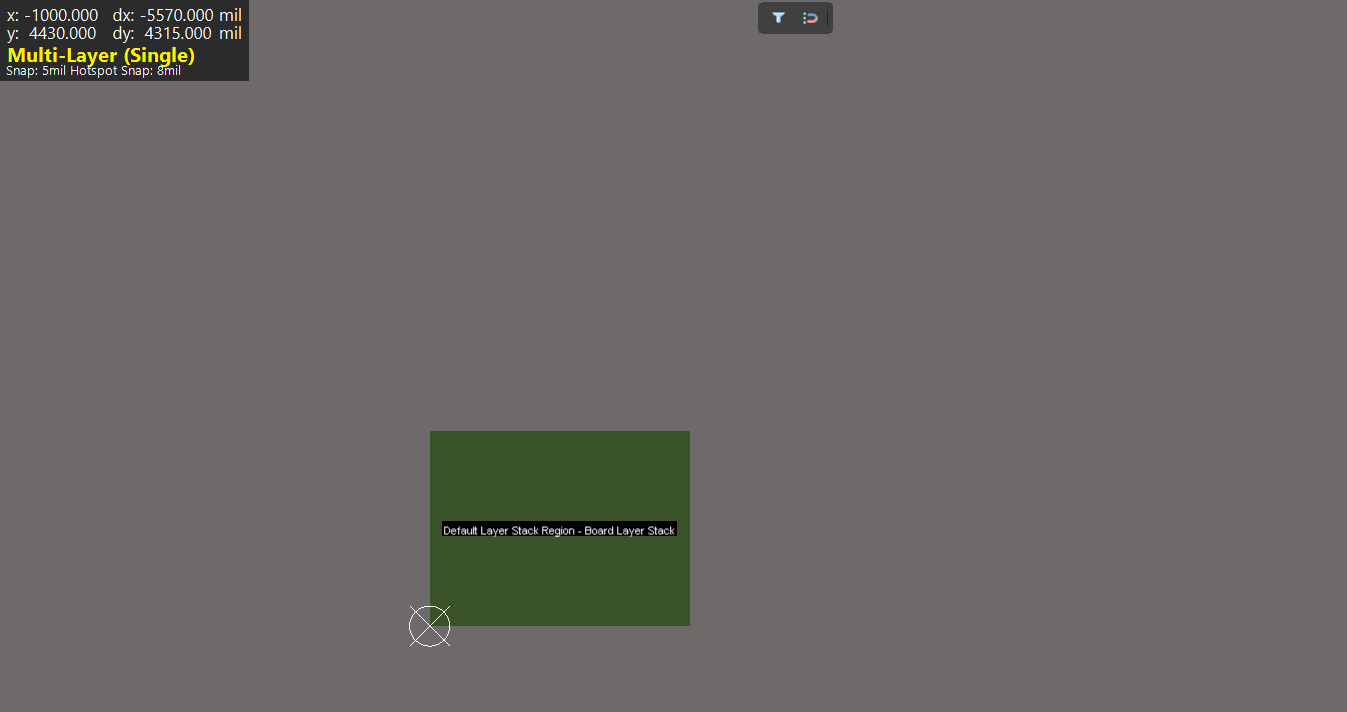
Once you're done, your board should be a much smaller shape.
[](https://wiki.soonerrobotics.org/uploads/images/gallery/2026-10/xwkimage.png)
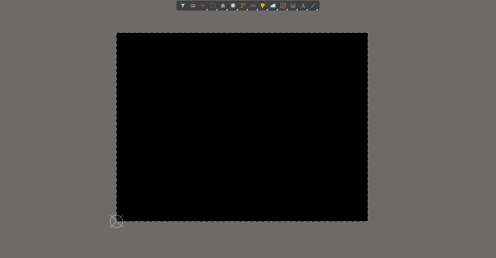
Navigate back to **2D Layout Mode** (toggle **View** in the toolbar) until you have something that looks like this:
[](https://wiki.soonerrobotics.org/uploads/images/gallery/2026-10/7LKimage.png)
## Layer Stack-Up
With your board size ready, we can check our layer stack-up manager. For PCB design, it's important to consider how many layers or "planes" you want on your board.
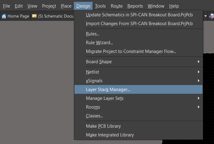
To view this, go to **Design** --> then select **Layer Stack Manager**.
[](https://wiki.soonerrobotics.org/uploads/images/gallery/2026-10/xZkimage.png)
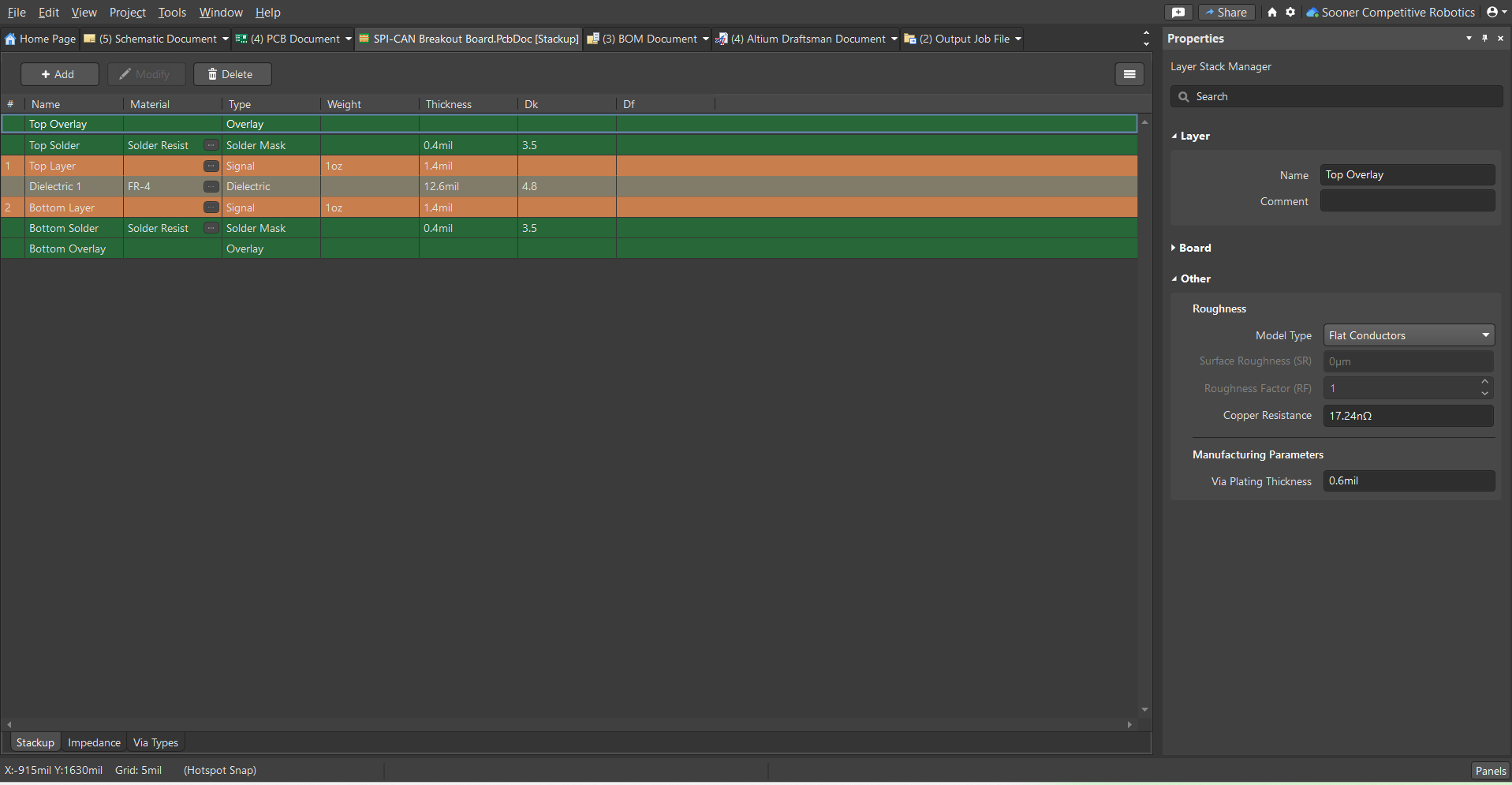
You should get a new window that looks like below:
[](https://wiki.soonerrobotics.org/uploads/images/gallery/2026-10/tkEimage.png)
In PCB Design, you can add more than two layers to a board. For our purposes, we'll leave the the design at two layers. If you wanted to add more layers, this is where you can add them.
## Design Rules
For the Design Rule Check, it's important to ensure the constraints we're applying to our layout are realistic and meet the requirements of our components. For our design, we want to modify the rules due to component pad sizes.
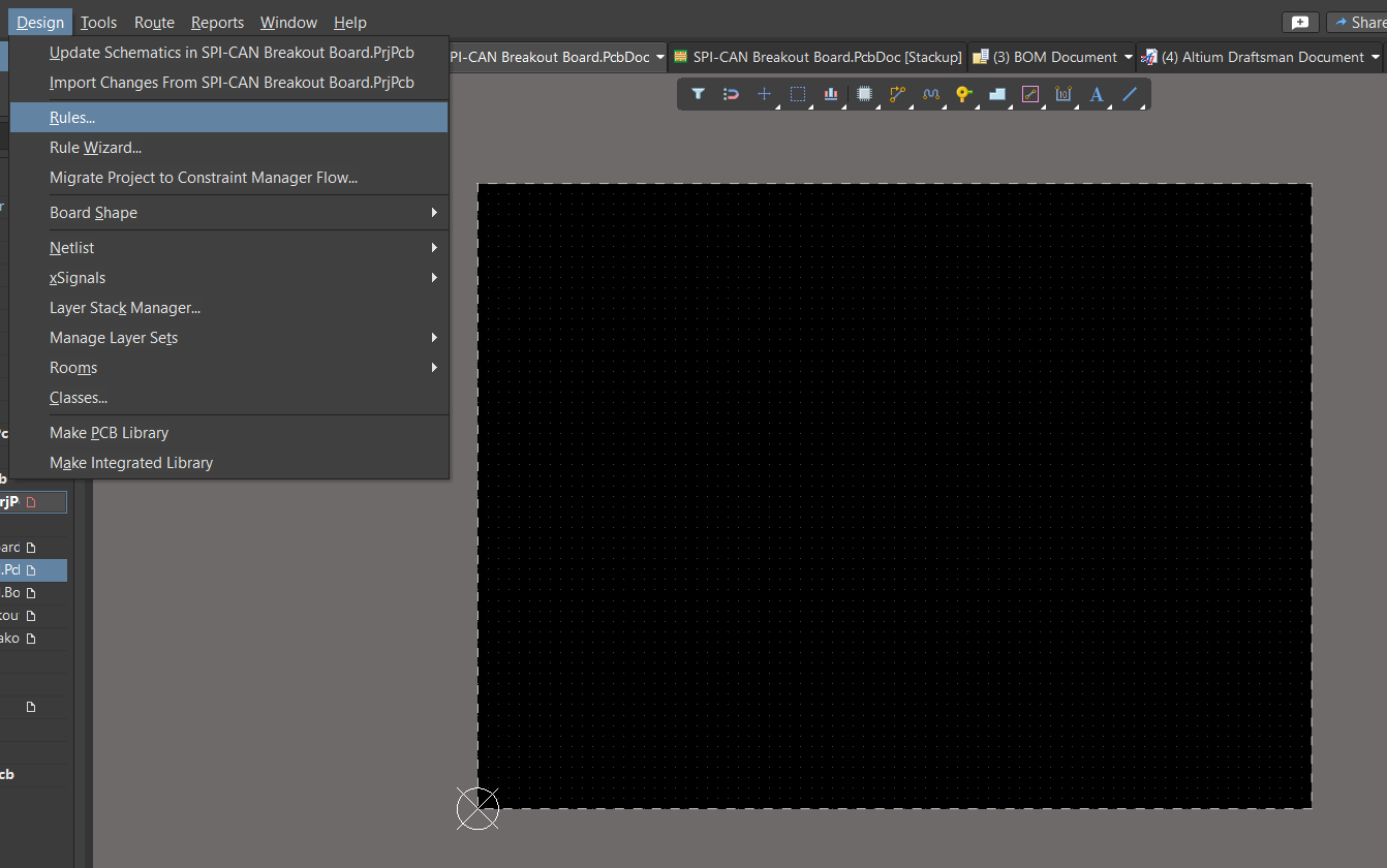
To start, navigate to the top left tool-bar and select **Design** --> then select **Rules**
[](https://wiki.soonerrobotics.org/uploads/images/gallery/2026-10/O5yimage.png)
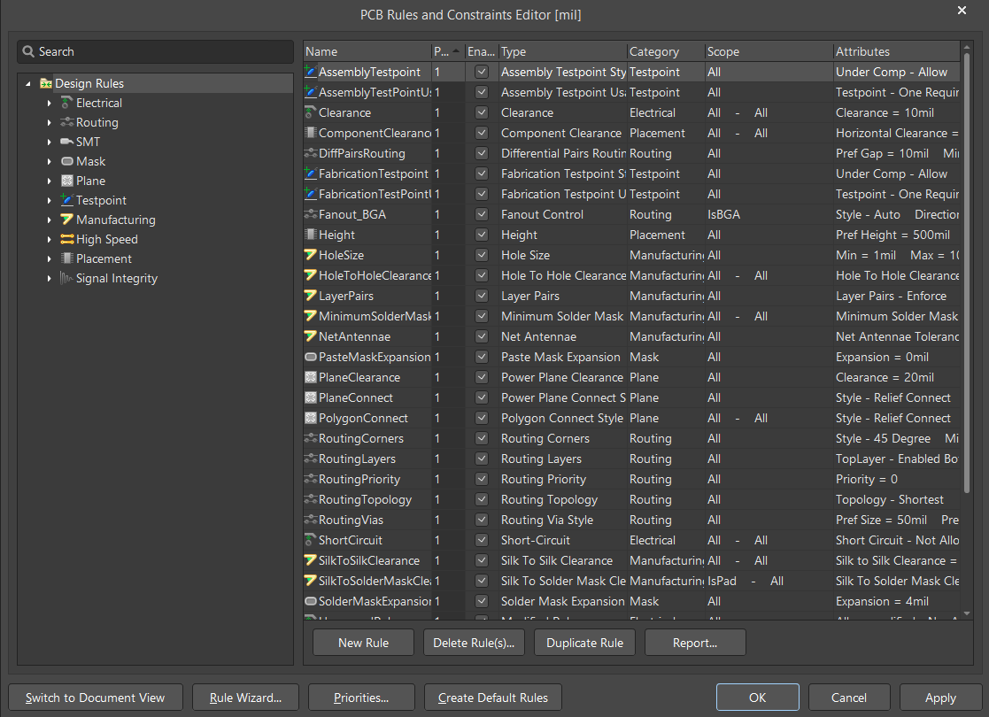
You'll be greeted by a new window with a ton of different constraints you can apply to your design.
[](https://wiki.soonerrobotics.org/uploads/images/gallery/2026-10/cmVimage.png)
For our design, we want to modify the following rules:
1. Trace Width Constraint
2. Hole Size Constraint
3. Polygon Connect
4. Silk to Solder Mask Clearance
#### Trace Width Constraint
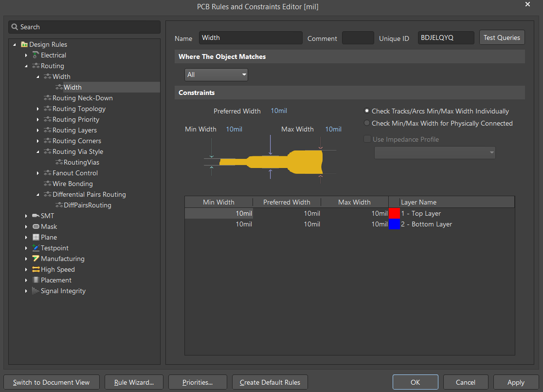
Open the drop-down options on the left side of the window until you reach the following page **(Routing** --> **Width** --> **Width).**
[](https://wiki.soonerrobotics.org/uploads/images/gallery/2026-10/DyGimage.png)
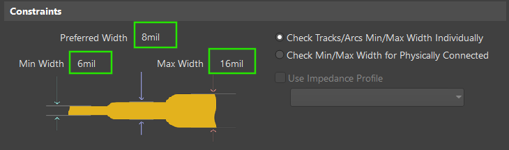
Modify the parameters under constraints to the following values:
- Min Width: 6 mil
- Preferred Width: 8 mil
- Max Width: 16 mil
[](https://wiki.soonerrobotics.org/uploads/images/gallery/2026-10/hJnimage.png)
#### Hole Size Constraint
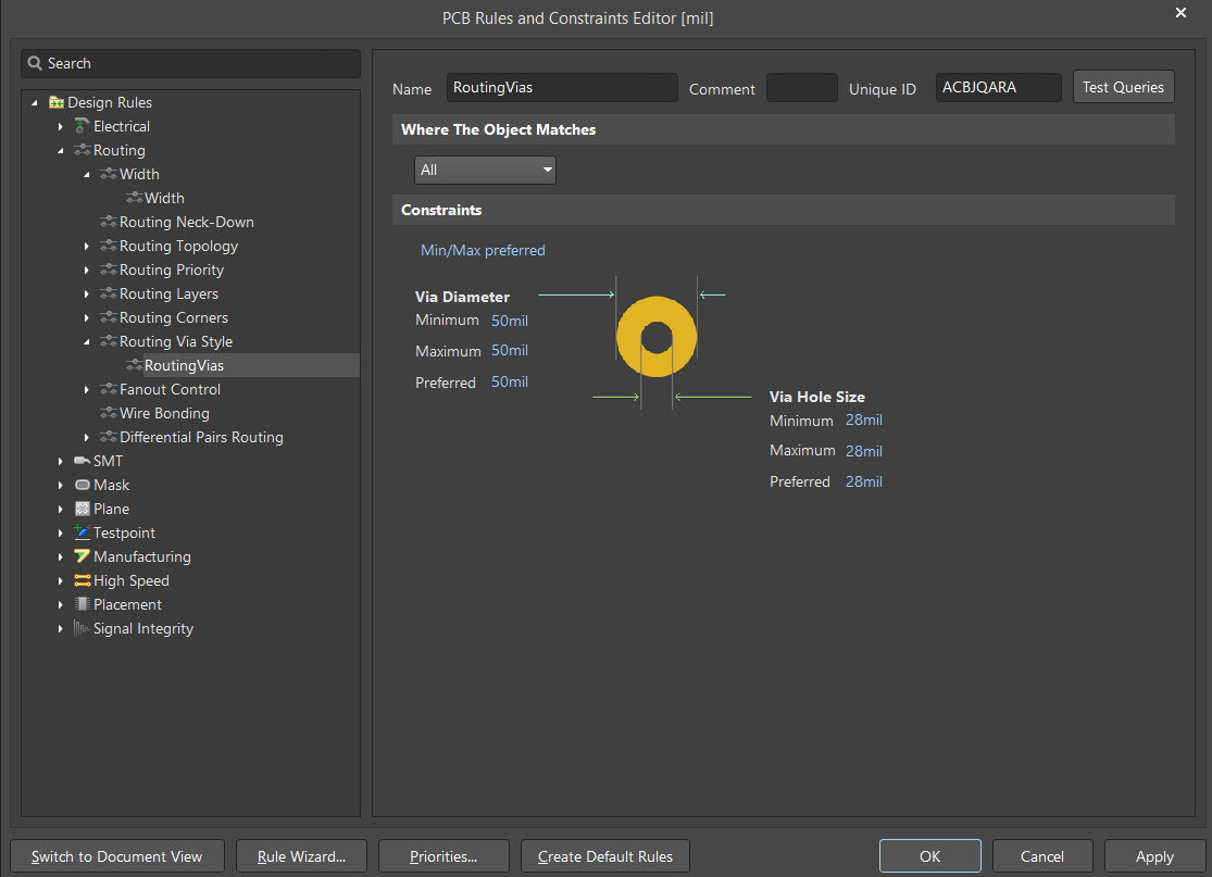
Next, navigate to the Routing Vias Page (**Routing** --> **Routing Via Style** --> **RoutingVias**)
[](https://wiki.soonerrobotics.org/uploads/images/gallery/2026-10/7bbimage.png)
Modify the parameters under the Constraints tab until you have the following values:
|
| Via Diameter: | Via Hole Size |
| Minimum | 20mil | 10mil |
| Maximum | 50mil | 20mil |
| Preferred | 25mil | 12mil |
[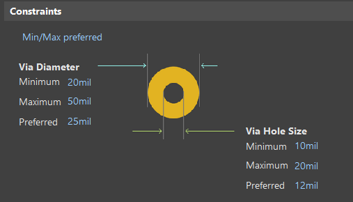](https://wiki.soonerrobotics.org/uploads/images/gallery/2026-10/ifqimage.png)
Next, navigate to the HoleSize module (**Manufacturing** --> **Hole Size** --> **HoleSize**).
[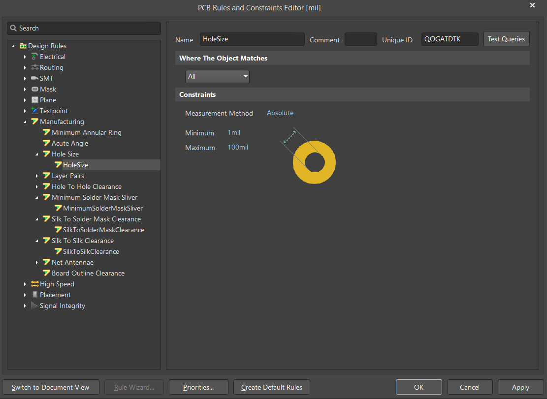](https://wiki.soonerrobotics.org/uploads/images/gallery/2026-10/xrHimage.png)
Modify the **Maximum** parameter to **300mil**.
[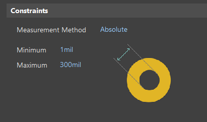](https://wiki.soonerrobotics.org/uploads/images/gallery/2026-10/0JDimage.png)
#### Polygon Connect
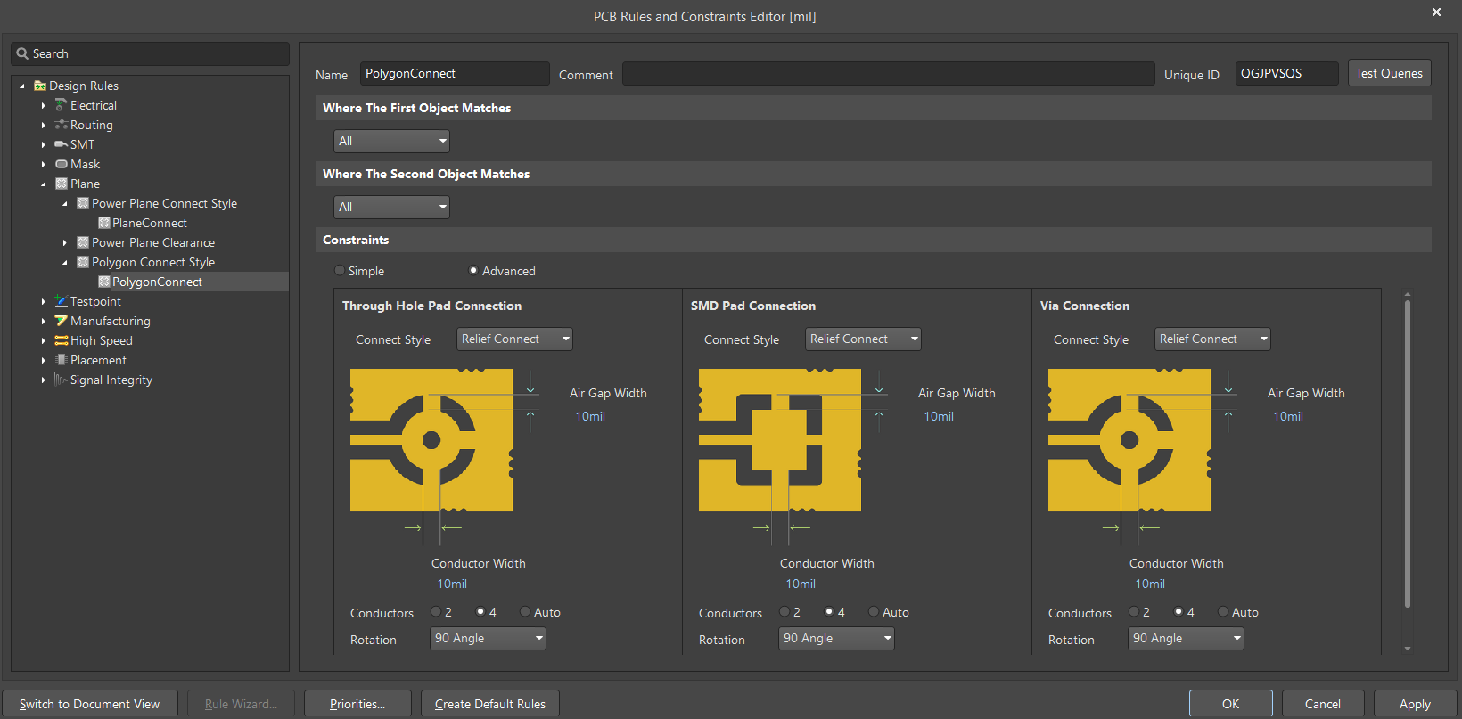
Now, we need to change the polygon connect rules. For our power and ground Vias, we want to ensure they have easy access to their respective signals going in and out of their connected planes.
To do this, navigate to the Polygon Connect module (**Plane** -> **Polygon ConnectStyle** --> **PolygonConnect**).
[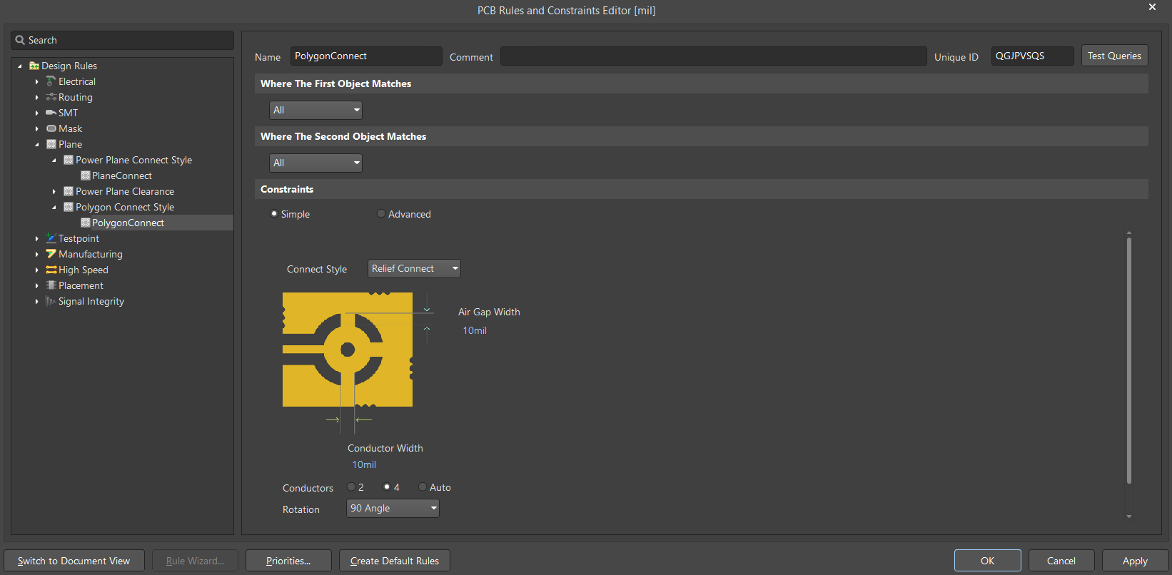](https://wiki.soonerrobotics.org/uploads/images/gallery/2026-10/Fcbimage.png)
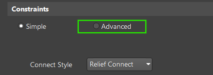
Under **Constraints**, toggle on the **Advanced** option.
[](https://wiki.soonerrobotics.org/uploads/images/gallery/2026-10/EbPimage.png)
You should have a view of the full page.
[](https://wiki.soonerrobotics.org/uploads/images/gallery/2026-10/wojimage.png)
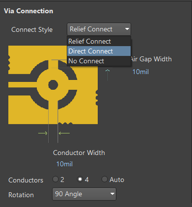
Now, under **Via Connection**, change the **Connect Style** to **Direct Connect**.
[](https://wiki.soonerrobotics.org/uploads/images/gallery/2026-10/Rnqimage.png)
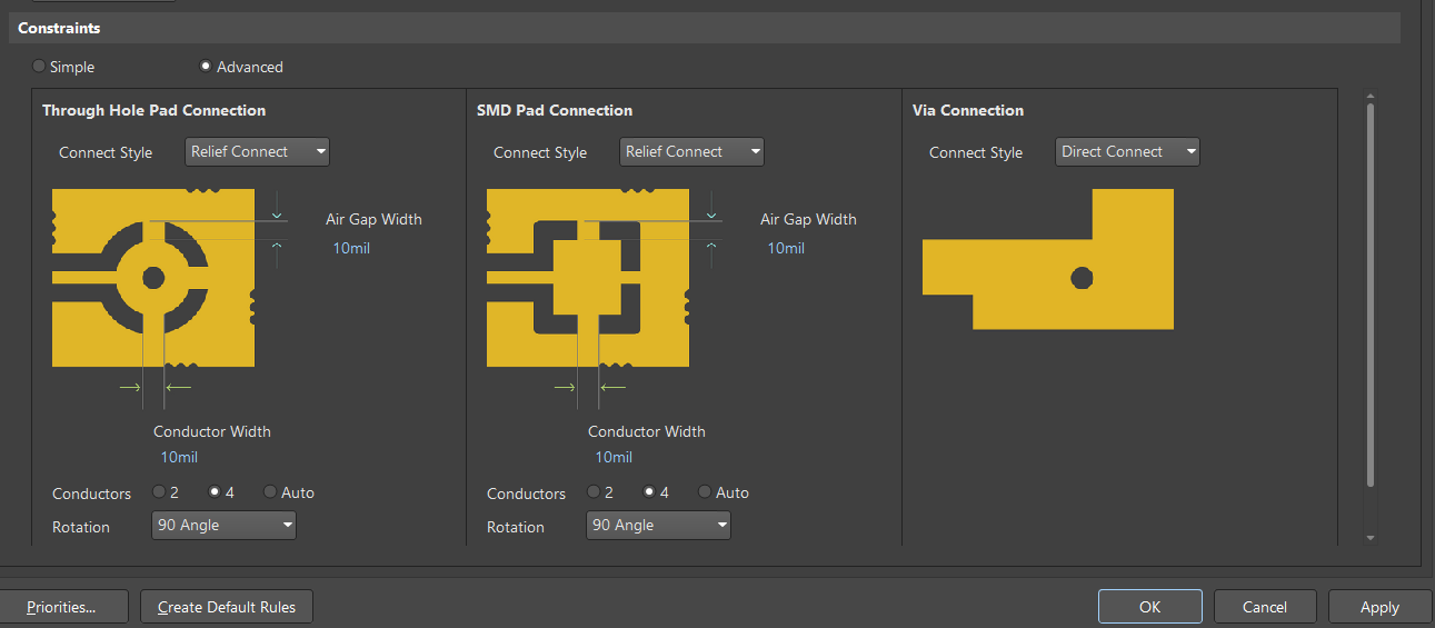
Your page should now look like what's seen below:
[](https://wiki.soonerrobotics.org/uploads/images/gallery/2026-10/x8Simage.png)
#### Silk to Solder Mask Clearance
Finally, we need to modify the clearance constraint between the silk and solder mask. Navigate to the window below (**Manufacturing** --> **Silk To Solder Mask Clearance** --> **SilkToSolderMaskClearance**).
[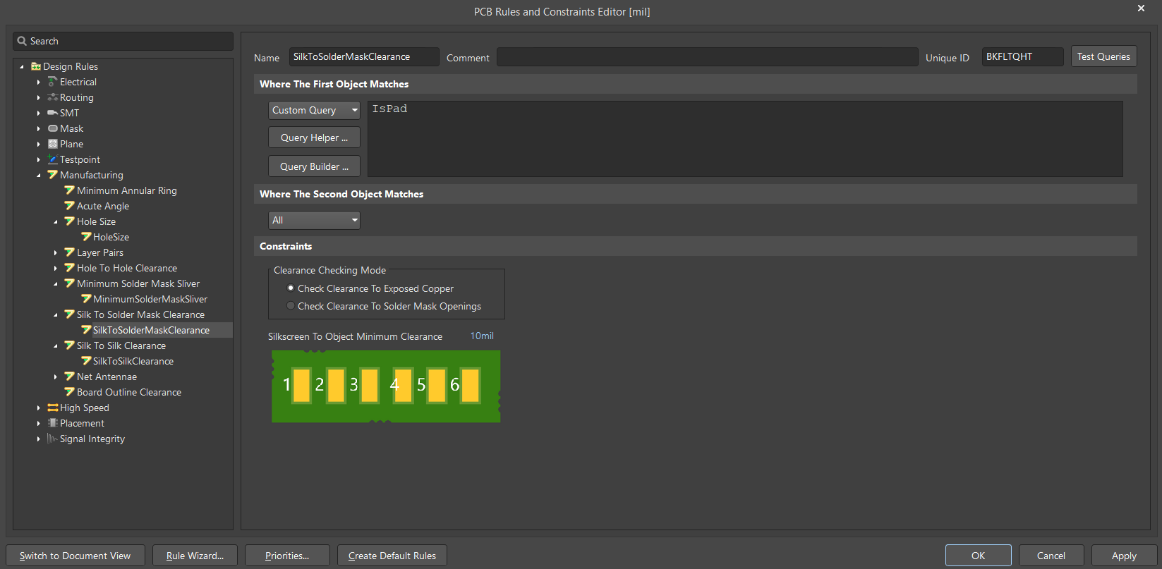](https://wiki.soonerrobotics.org/uploads/images/gallery/2026-10/RPiimage.png)
Change the **Silkscreen to Object Minimum Clearance** parameter to **4mil**.
[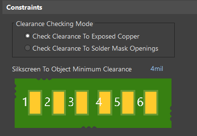](https://wiki.soonerrobotics.org/uploads/images/gallery/2026-10/Na9image.png)
#### Finalizing Design Rules
Once you have all the rule constraints set to your needs, select the **Apply** option on the bottom right of the window. Then select **OK**.
[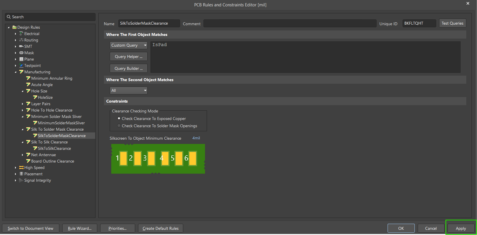](https://wiki.soonerrobotics.org/uploads/images/gallery/2026-10/8P8image.png)
This concludes our section on the layout set-up. To continue to the next part of the layout tutorial, navigate to this page: [4. Layout Pt. II](https://wiki.soonerrobotics.org/books/pcb-design-altium-how-to/page/4-board-layout-pt-ii)
####
# 4. Board Layout Pt. II
> *Before you begin, this tutorial assumes you completed part I of the layout tutorial. You can find the tutorial by accessing this page: [3. Board Layout Pt. I](https://wiki.soonerrobotics.org/books/pcb-design-altium-how-to/page/3-board-layout-pt-i)*
## Component Placement
Before you can place your components, you must import your parts from the schematic you created. To import your components, navigate to the top left tool-bar, select **Design** --> then select **Import Changes From SPI-CAN Breakout Board.PrjPCb**.
[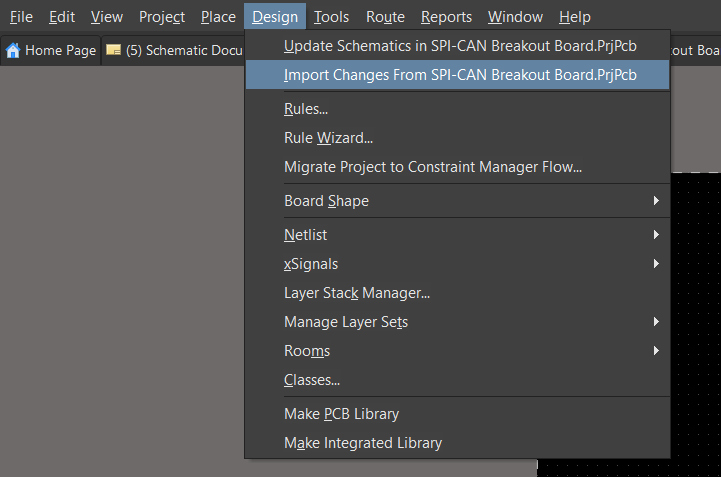](https://wiki.soonerrobotics.org/uploads/images/gallery/2026-10/CHsimage.png)
A new window will appear showcasing which components and nets will be added to the layout.
[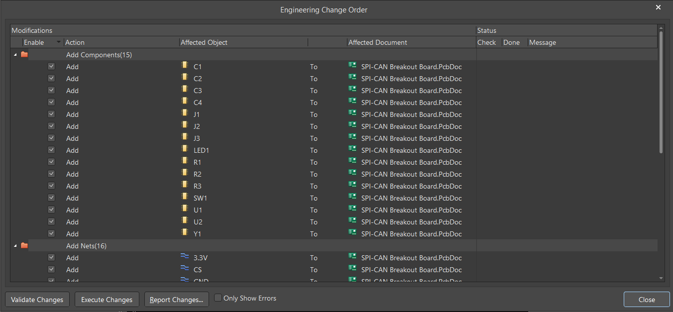](https://wiki.soonerrobotics.org/uploads/images/gallery/2026-10/csCimage.png)
Go ahead and select **Validate Changes**, then select **Execute Changes**. Green checkmarks will appear under the **Check** and **Done** columns, indicating if a component has been successfully imported.
[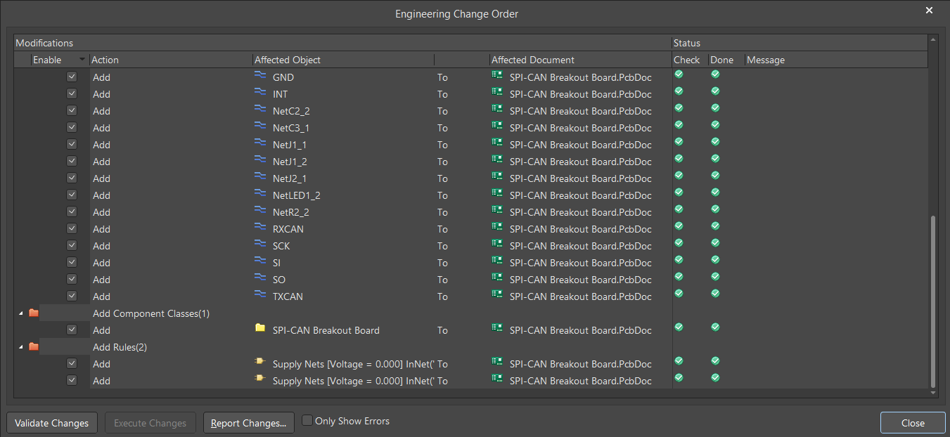](https://wiki.soonerrobotics.org/uploads/images/gallery/2026-10/u2Ximage.png)
Upon closing the window, your components will appear on the layout as shown below:
[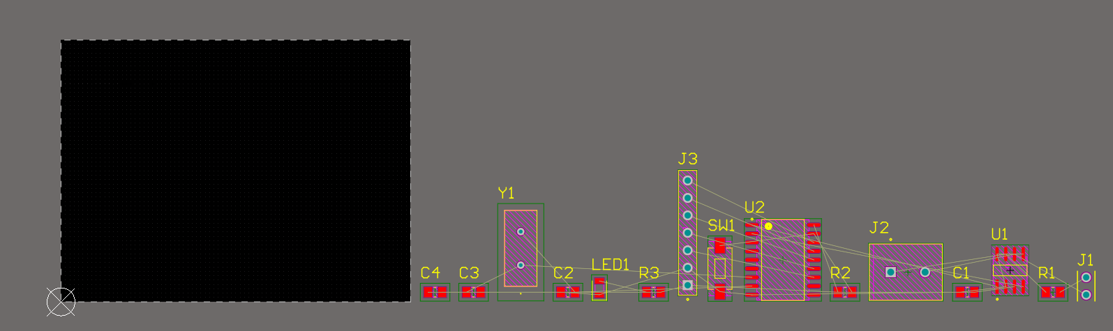](https://wiki.soonerrobotics.org/uploads/images/gallery/2026-10/4FKimage.png)
Typically, you can click and drag components into your board perimeter. For the sake of time, we'll use a different technique for placing components by having our schematic and PCB documents open side-by-side.
Start by having only two windows open: your schematic and your PCB documents.
[](https://wiki.soonerrobotics.org/uploads/images/gallery/2026-10/4CXimage.png)
To close a window, right-click on the window you want to close, then select **Close \[Window Name\]**
[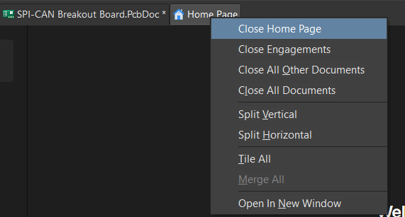](https://wiki.soonerrobotics.org/uploads/images/gallery/2026-10/EOwimage.png)
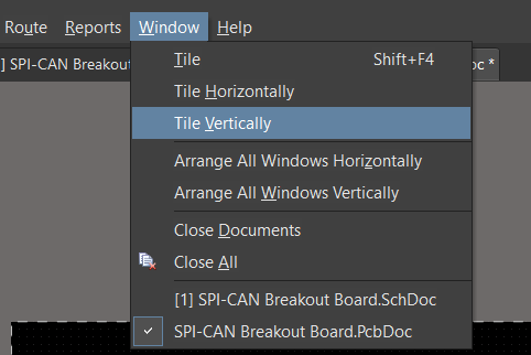
Next, navigate to the toolbar on the top left of your screen, select **Window** --> then select **Tile Vertically**.
[](https://wiki.soonerrobotics.org/uploads/images/gallery/2026-10/ITYimage.png)
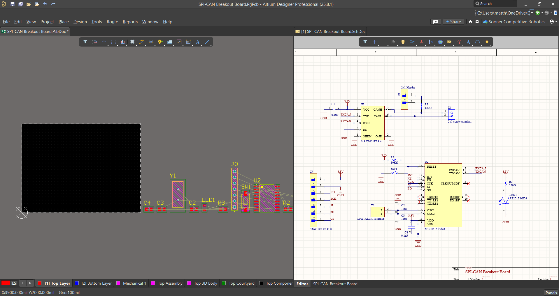
Now, your Layout and Schematic should appear side-by-side one another.
[](https://wiki.soonerrobotics.org/uploads/images/gallery/2026-10/6ynimage.png)
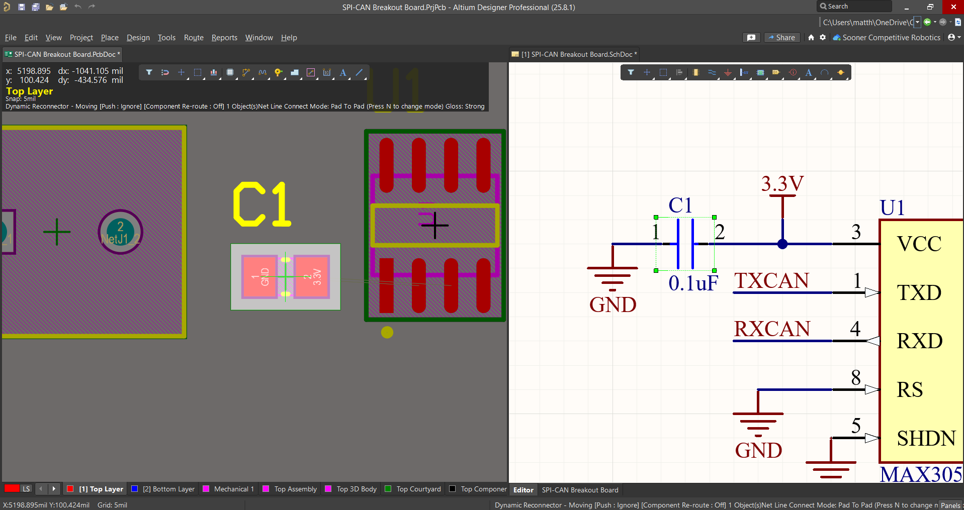
This way, by selecting a part on the schematic, Altium will automatically select the same part on the PCB layout.
[](https://wiki.soonerrobotics.org/uploads/images/gallery/2026-10/kfAimage.png)
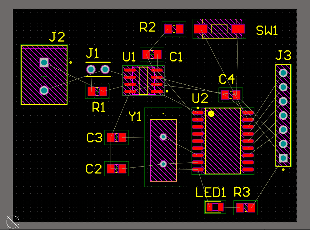
Using this technique, arrange the components on the layout as seen below. Remember, there's multiple ways to conduct this layout, this is just one of the solutions.
[](https://wiki.soonerrobotics.org/uploads/images/gallery/2026-10/R5Jimage.png)
> *Note: in layout design, it's important to keep "friendly" components close together for high functionality. I.e., keep your decoupling capacitors close to the device they're decoupling, etc.*
## Layout Routing
Once you have your components arranged, you'll start wiring your components together through tracing.
Tracing is connecting solder masks together on a PCB using thin copper lines. These lines carry current between your components. Think of them as flat wires on your board.
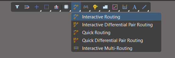
To trace your components together, you have a couple of options. First, you can navigate to the toolbar with the various icons, right-click on the middle icon (the diagonal line with the arrow), then select **Interactive Routing**.
- Another way to access the trace feature is by holding **Ctrl + W** on your keyboard.
[](https://wiki.soonerrobotics.org/uploads/images/gallery/2026-10/QAJimage.png)
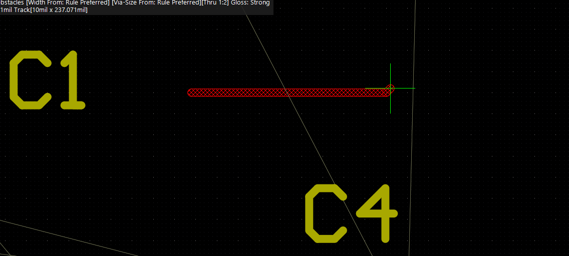
A green cross will now appear with your cursor. When you left-click on your layout, a red line will appear from the spot your selected. This creates a faded trace waiting to be place.
[](https://wiki.soonerrobotics.org/uploads/images/gallery/2026-10/jb4image.png)
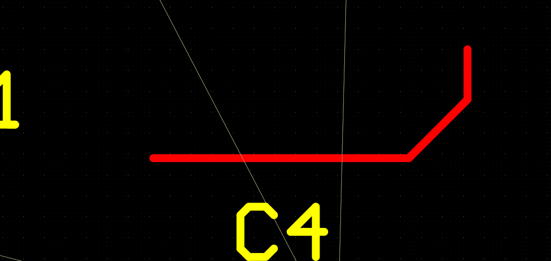
Upon left-clicking again, that part of the trace will be placed on the layout. From the second spot you selected, another part of the trace will begin appearing. To finish placing the trace, press **esc** on your keyboard.
[](https://wiki.soonerrobotics.org/uploads/images/gallery/2026-10/2Wzimage.png)
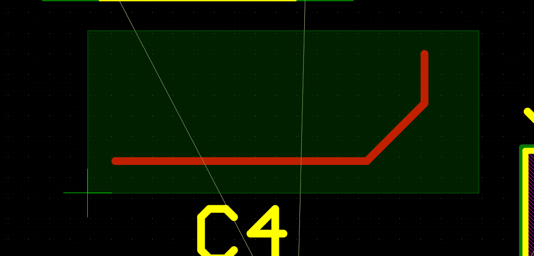
Since this trace is floating, we don't need it for our design. To delete a trace, select the entire trace by holding down left-click and highlighting the entire object. Then, select **delete** on your keyboard.
[](https://wiki.soonerrobotics.org/uploads/images/gallery/2026-10/9DCimage.png)
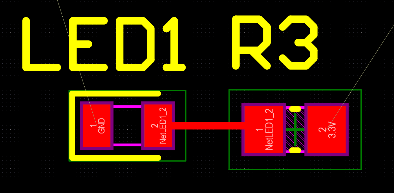
Let's practice connecting a trace between two pins. Navigate to the bottom of the layout and find **LED1** and **R3**.
[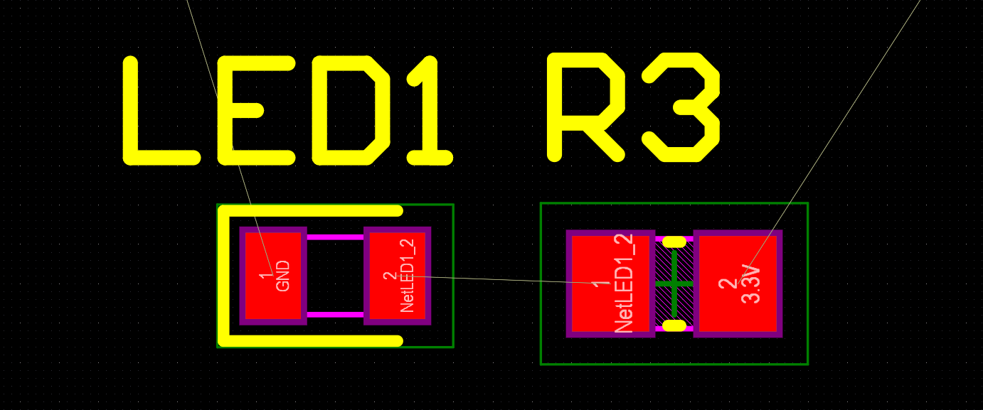](https://wiki.soonerrobotics.org/uploads/images/gallery/2026-10/9Eaimage.png)
We'll route these two components together. Notice how there are thin gray lines connecting between pins of specific components. These thin lines tell you which pins need to be routed together. If you Zoom in on a component, you can read the Net associated with it's pins.
Between LED3 and R3, we see they both have the **LED1\_2** net.
[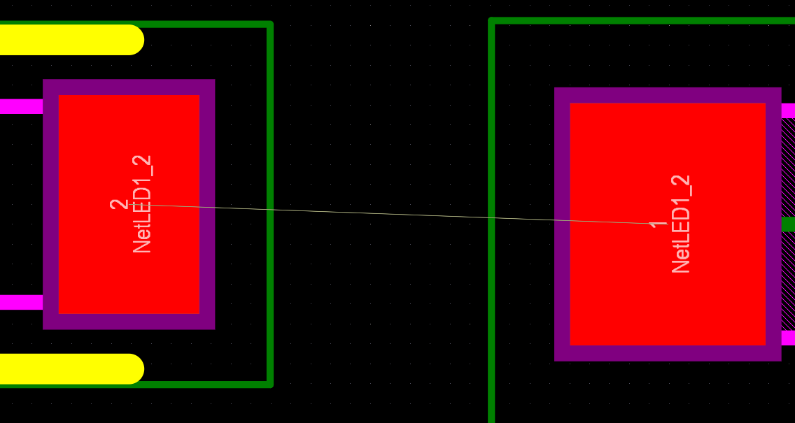](https://wiki.soonerrobotics.org/uploads/images/gallery/2026-10/5SJimage.png)
To trace these pins together, activate the routing tool. Then place the start of your trace on either pad. You'll notice when you hover over the center of a pin, your cursor will snap onto the center with a green cross hair.
[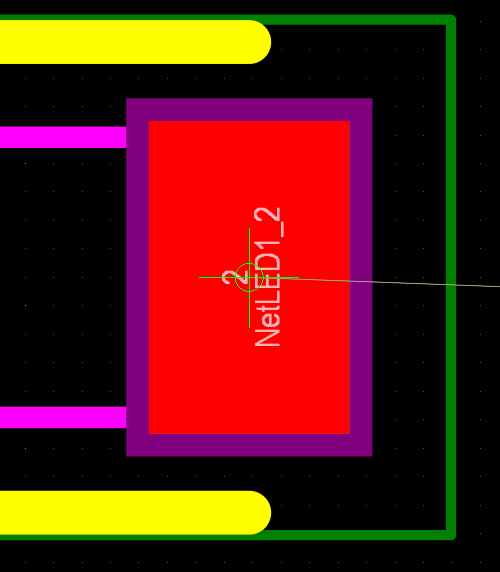](https://wiki.soonerrobotics.org/uploads/images/gallery/2026-10/EDRimage.png)
Now, drag your trace across the layout onto the second pin. You should get a faded trace like below:
[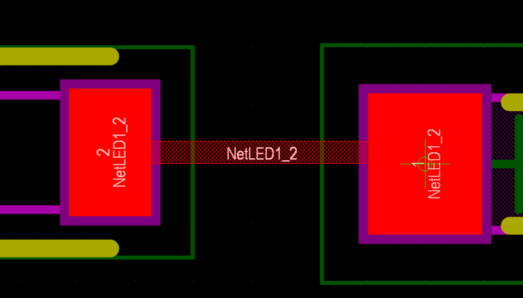](https://wiki.soonerrobotics.org/uploads/images/gallery/2026-10/MWDimage.png)
Left-click on the second pin whenever the cursor snaps over the center of the pad. Now, you should have a completed trace.
[](https://wiki.soonerrobotics.org/uploads/images/gallery/2026-10/OYaimage.png)
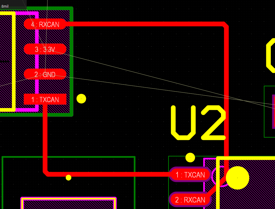
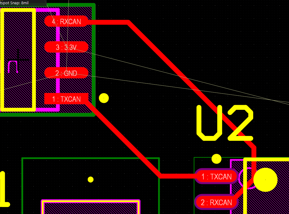
One thing to keep in mind when routing is to ensure your signals travel across the path of least resistance. This means setting up your traces at bends with 45 degree angles. A trace that bends at 90 degrees creates signal inflections in your design, causing increased electro-magnetic inteference (EMI) and impedance discontinuties (both bad things).
The picture on the right is a much better example of routing compared to the left.
[](https://wiki.soonerrobotics.org/uploads/images/gallery/2026-10/eINimage.png)
[](https://wiki.soonerrobotics.org/uploads/images/gallery/2026-10/iJbimage.png)
> *Note: in actual layout design, it's important to use differential pairing on signals that operate at the same frequency (For instance, signals TXCAN and RXCAN from U2). This can help mitigate issues with cross-talk and EMI. For our purposes, we won't consider this issue. But, keep this in mind for future designs!*
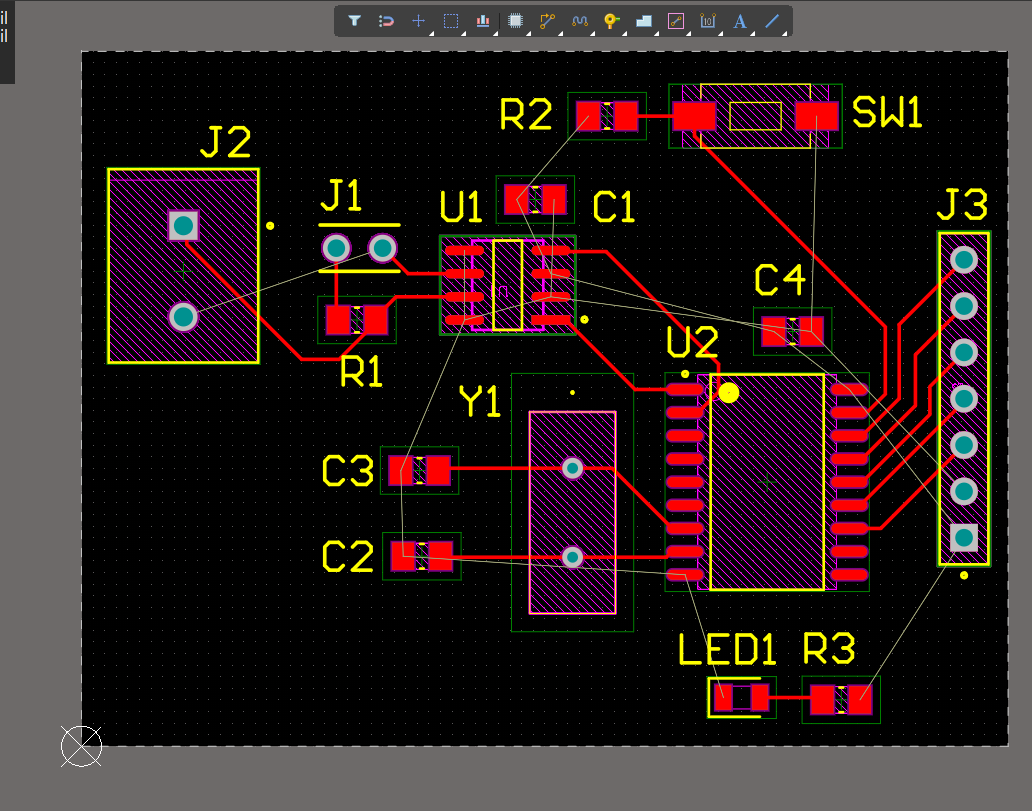
Now, use the techniques you just learned to conduct the routing between all of your signals nets as seen below:
[](https://wiki.soonerrobotics.org/uploads/images/gallery/2026-10/i6Fimage.png)
You can also route between signals on different layers of your board. For instance, let's route two pins on the bottom layer.
To do this, navigate to the bottom toolbar on your screen and select **Bottom** **Layer**.
[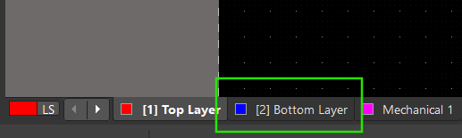](https://wiki.soonerrobotics.org/uploads/images/gallery/2026-10/iXWimage.png)
Next, route the **NetJ1\_2** signal between your **J1** and **J2** components. You'll see the trace appear in blue as seen below.
[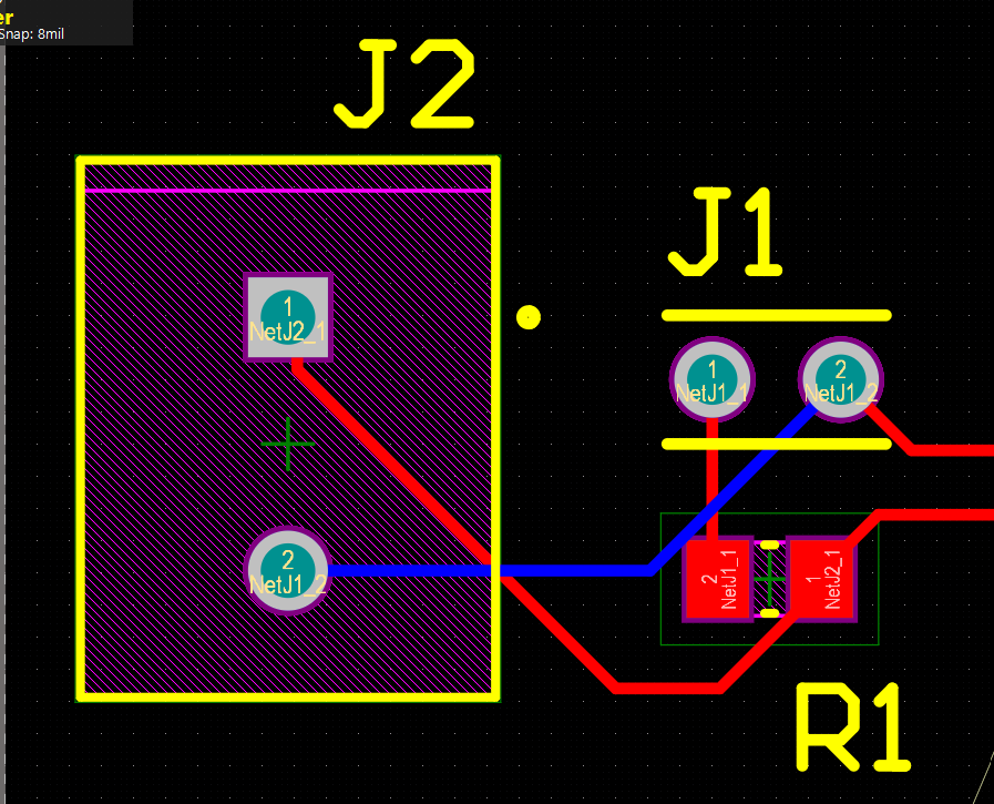](https://wiki.soonerrobotics.org/uploads/images/gallery/2026-10/67Himage.png)
Notice how the blue trace went under the red traces. This is extremely helpful if a pin you're routing is blocked by existing traces on the same layer.
> *Note: this only works easily for through-hole pins. Connecting a trace from another layer directly to a surface-mount component on a different layer (like R1) won't work! To avoid this, you'll need to place a routing via next to your pad before connecting a trace from another layer.*
## Fanout Vias
Vias are holes in a PCB with an inner coating of copper that carries signals between layers. A side profile of a via can be seen below as found in the Layer Stack Manager.
[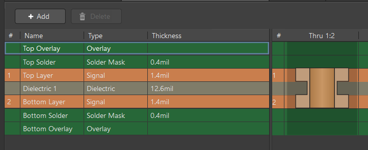](https://wiki.soonerrobotics.org/uploads/images/gallery/2026-10/R7kimage.png)
For all of our power pins, it's important to place a Via next to each 3.3V surface-mount pad to allow power to easily flow from the power plane to the pad.
To place a routing via, navigate to the top toolbar and right-click on the yellow circle icon, then select **Via**.
[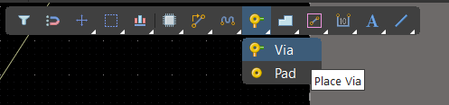](https://wiki.soonerrobotics.org/uploads/images/gallery/2026-10/V9Mimage.png)
A faded via should now appear with your cursor. Left-click anywhere on the layout to place your via.
[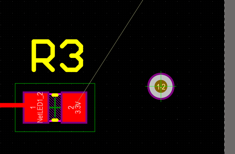](https://wiki.soonerrobotics.org/uploads/images/gallery/2026-10/iUTimage.png)
Double left-click on the via. In the Properties window, update the parameters to the following values:
- Net: 3.3V
- Diameter: 30mil
- Hole Size: 20mil
- Thermal Relief: Direct Enabled
[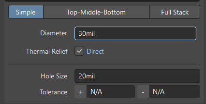](https://wiki.soonerrobotics.org/uploads/images/gallery/2026-10/ObSimage.png)
Under Solder Mask Expansion, select the **Manual** tab, then selected **Tented** for the Top and Bottom dialogs.
[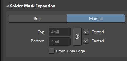](https://wiki.soonerrobotics.org/uploads/images/gallery/2026-10/kFgimage.png)
> *Note: Enabling the Tented option will embed your via into the board, preventing you from applying solder to the via!*
After you update the via's parameters, your fanout via should look much smaller.
[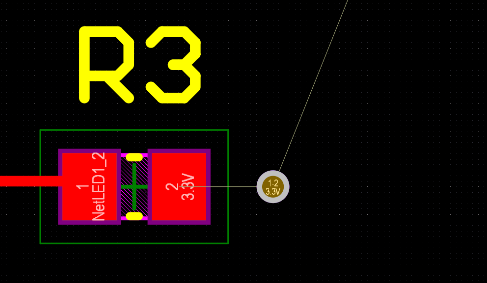](https://wiki.soonerrobotics.org/uploads/images/gallery/2026-10/TFuimage.png)
Next, connect a trace between R3's 3.3V pad and the fanout via you just created. Make sure to keep the fanout via close to the pad.
[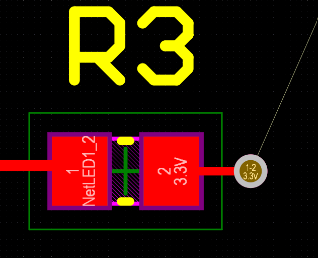](https://wiki.soonerrobotics.org/uploads/images/gallery/2026-10/WcWimage.png)
Go ahead and copy & paste your new fanout via, and attach it to every surface-mount 3.3V pad. You should have 5 total on your board.
Once you're done, your layout should be similar to below:
[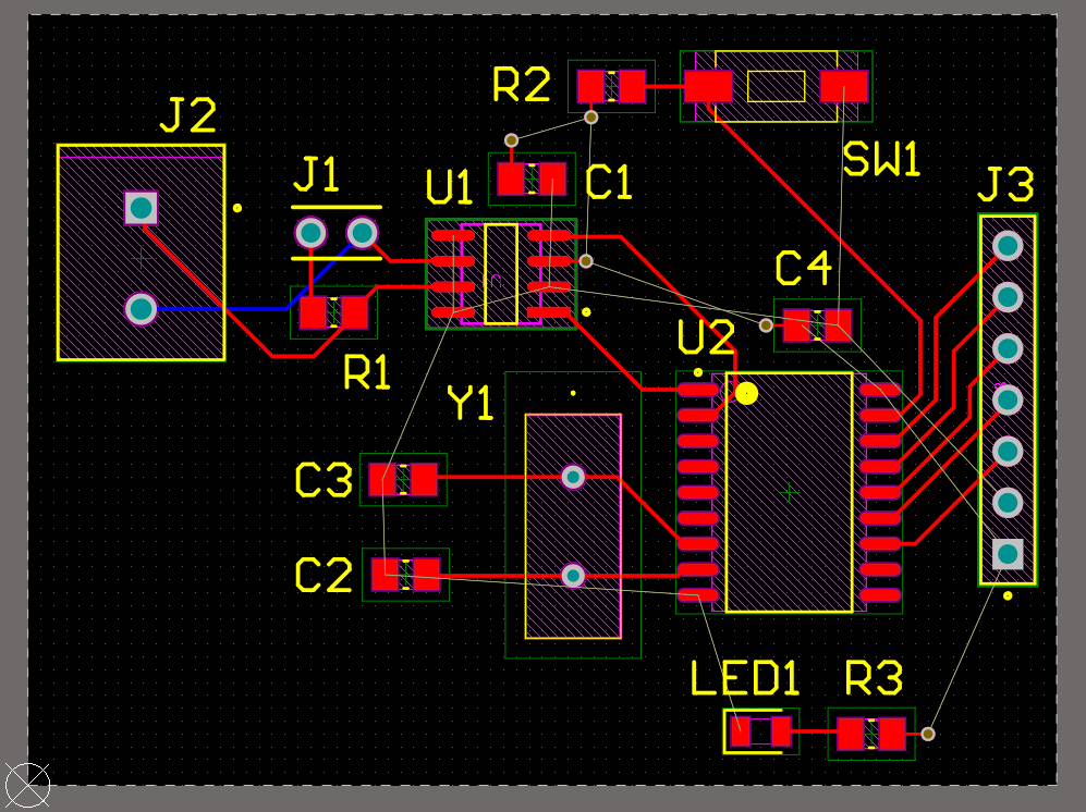](https://wiki.soonerrobotics.org/uploads/images/gallery/2026-10/aRtimage.png)
## Mounting Holes
When we install a PCB on the robot, it's important to have screw holes readily implemented onto the board to allow the Mech-E subteam to use our boards.
To start, rearrange the board slightly to make room for the mounting holes:
[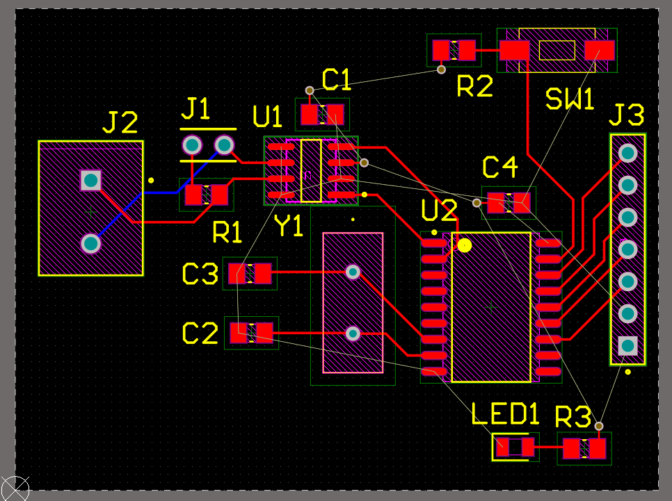](https://wiki.soonerrobotics.org/uploads/images/gallery/2026-10/Qi3image.png)
To place a mounting hole, navigate to the top toolbar, right-click on the via icon, then select **Pad**.
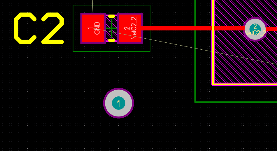
[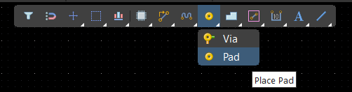](https://wiki.soonerrobotics.org/uploads/images/gallery/2026-10/zDdimage.png)
Place down your Pad. You should have something like below.
[](https://wiki.soonerrobotics.org/uploads/images/gallery/2026-10/JLCimage.png)
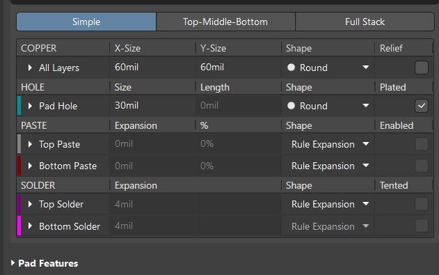
Open the Properties window for your pad. Navigate down to the **Pad Stack** module until you see the following table.
[](https://wiki.soonerrobotics.org/uploads/images/gallery/2026-10/uThimage.png)
Update the parameters to the following values:
|
| X-Size | Y-Size |
| All Layers | 100mil | 100mil |
| Pad Hole | 120mil |
|
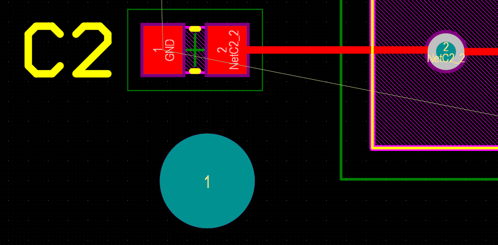
Your pad should now look like this.
[](https://wiki.soonerrobotics.org/uploads/images/gallery/2026-10/wptimage.png)
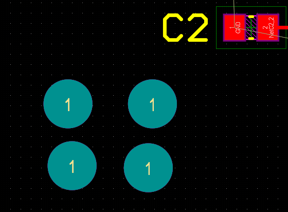
Copy and paste the mounting hole until you have four pads on the layout.
[](https://wiki.soonerrobotics.org/uploads/images/gallery/2026-10/QVYimage.png)
Open the Properties window for one of the Pads. Navigate down to the **(X/Y)** dialog boxes.
[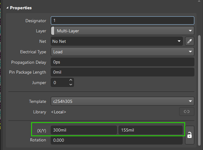](https://wiki.soonerrobotics.org/uploads/images/gallery/2026-10/Cwsimage.png)
For each of the pads, distribute the following coordinates:
| Pad | X (mil) | Y (mil) |
| 1 | 200 | 250 |
| 2 | 1200 | 250 |
| 3 | 200 | 1250 |
| 4 | 1200 | 1250 |
Your board should now look like the following:
[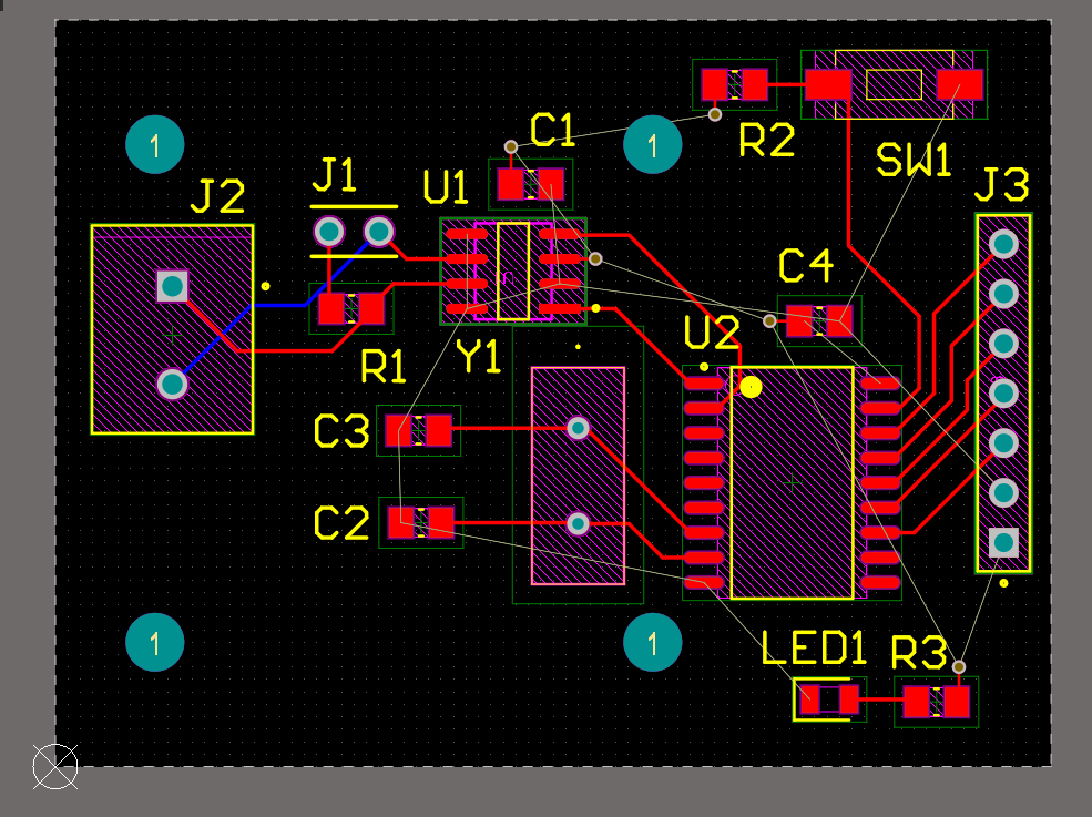](https://wiki.soonerrobotics.org/uploads/images/gallery/2026-10/A0Iimage.png)
## Polygon Pours
Now that you have your board traced, it's time to place down your polygon pours. Polygon pours are your board's layers. Each layer can contain a specific net, allowing you to creating power and ground planes. These planes will remove the final thin gray lines coming out from the power and ground pins.
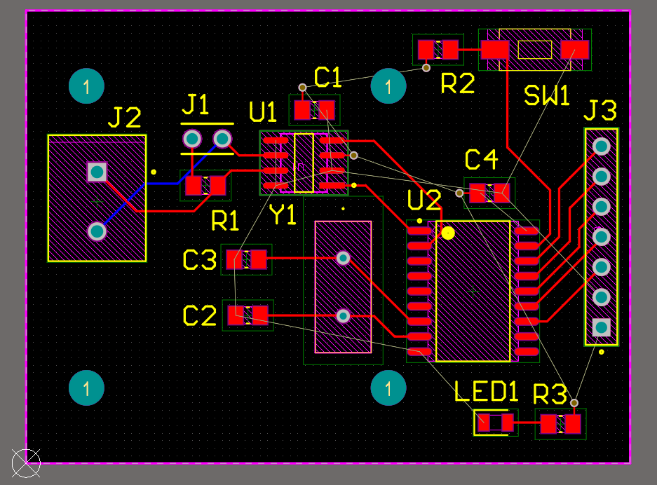
Before starting, place a red perimeter of traces around the edge of your board.
[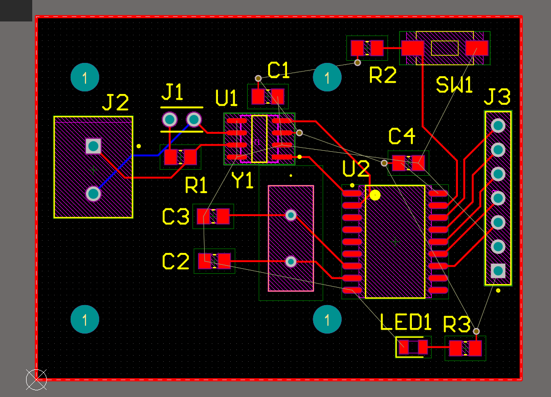](https://wiki.soonerrobotics.org/uploads/images/gallery/2026-10/PnDimage.png)
Select all the perimeter traces, then open the Properties window. Under Properties, change the width to **10mil** and the Net to **Mechanical 1.**
[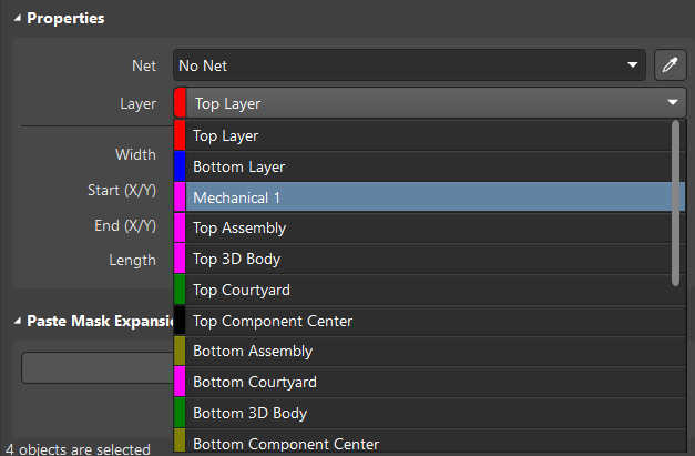](https://wiki.soonerrobotics.org/uploads/images/gallery/2026-10/e2kimage.png)
This border will help make it easier to create the Polygon Pours
[](https://wiki.soonerrobotics.org/uploads/images/gallery/2026-10/M1iimage.png)
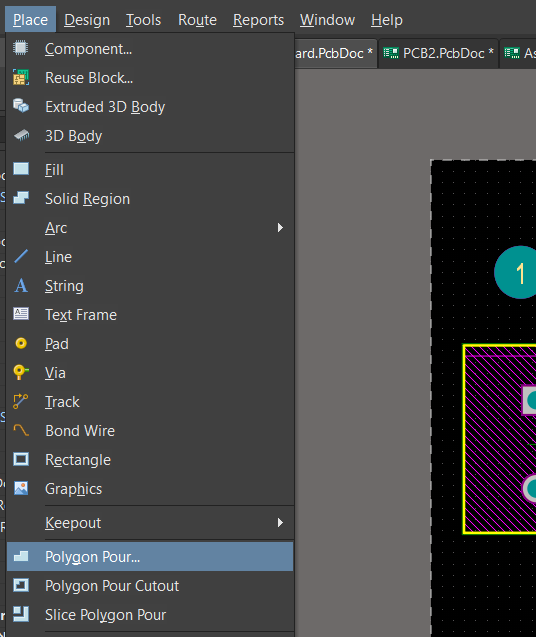
To create a polygon pour, Navigate to the top left tool-bar, select **Place** --> then select **Polygon Pour**.
[](https://wiki.soonerrobotics.org/uploads/images/gallery/2026-10/r7Oimage.png)
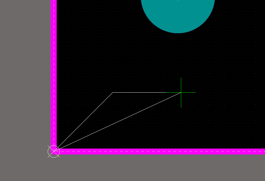
With your cursor, navigate to the bottom left corner of the board. Select the corner and drag your cursor until a triangle shape enlarges.
[](https://wiki.soonerrobotics.org/uploads/images/gallery/2026-10/Rhrimage.png)
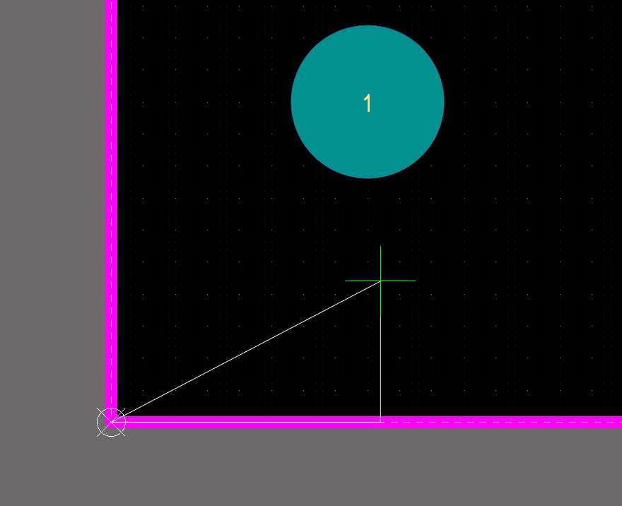
To change the polygon's shape, press **Shift + Space** until you get a right triangle. You can also press **Space** to flip the polygon.
[](https://wiki.soonerrobotics.org/uploads/images/gallery/2026-10/zrrimage.png)
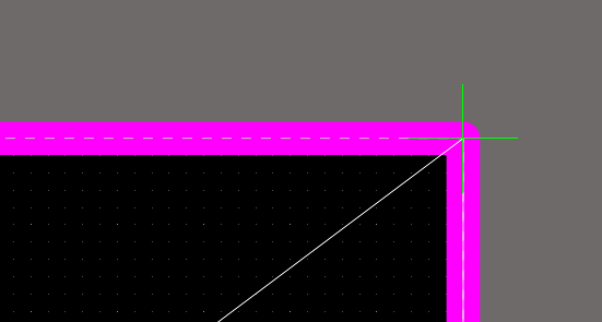
Next, head to the oppostie corner (top right) and place down the pour by left-clicking on the corner.
[](https://wiki.soonerrobotics.org/uploads/images/gallery/2026-10/z63image.png)
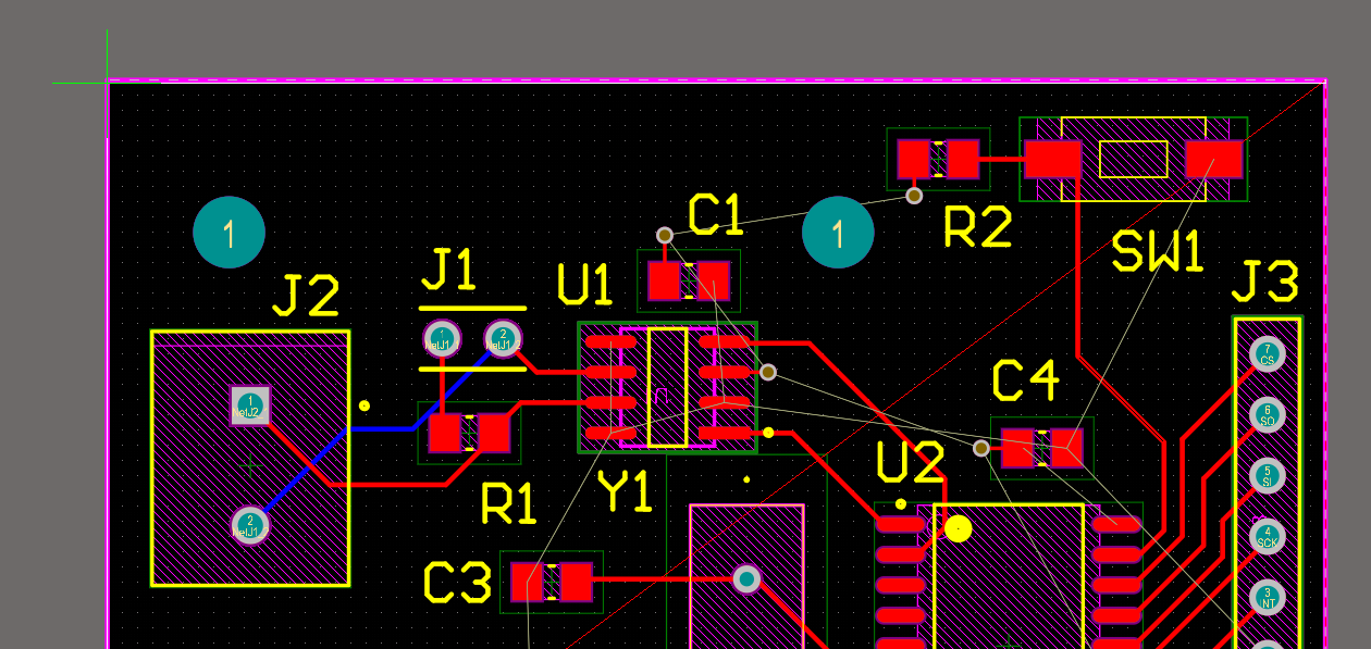
Finally, head to the last corner (top left) and place the last piece of your polygon.
[](https://wiki.soonerrobotics.org/uploads/images/gallery/2026-10/zeTimage.png)
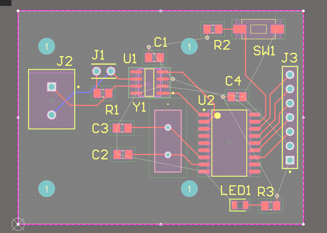
Now, you should have a placed polygon without a net. As a result, your polygon won't have any effect on your board.
[](https://wiki.soonerrobotics.org/uploads/images/gallery/2026-10/b4mimage.png)
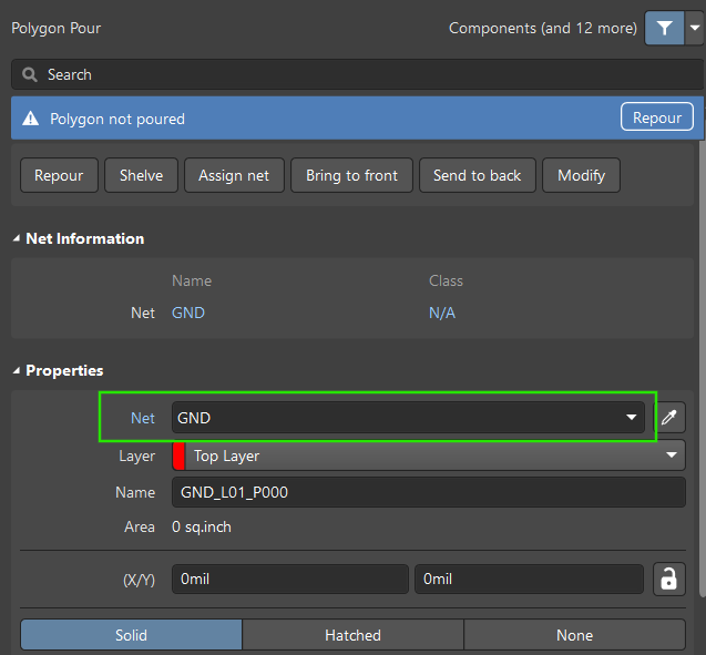
To fix this, open the Properties window for your polygon. Then, change the net to **GND** and **Repour** the Polygon.
[](https://wiki.soonerrobotics.org/uploads/images/gallery/2026-10/XXNimage.png)
Your board should now be filled with your GND-planed polygon.
[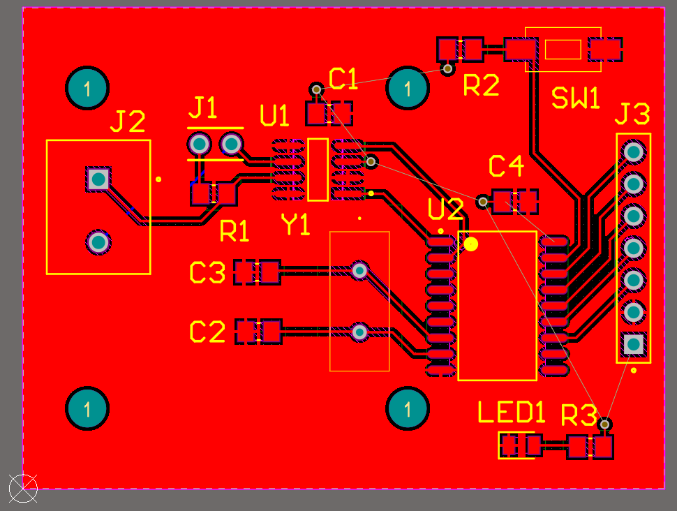](https://wiki.soonerrobotics.org/uploads/images/gallery/2026-10/G9simage.png)
Notice how the GND pads and vias are connecting to the GND plane you just created.
[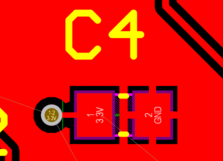](https://wiki.soonerrobotics.org/uploads/images/gallery/2026-10/FZnimage.png)
Now, let's create a polygon pour for our bottom layer. To do this, navigate to the top left tool-bar, select **Tools** --> select **Polygon Pours** --> then select **Polygon Manager**.
[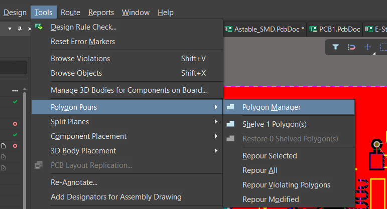](https://wiki.soonerrobotics.org/uploads/images/gallery/2026-10/KeBimage.png)
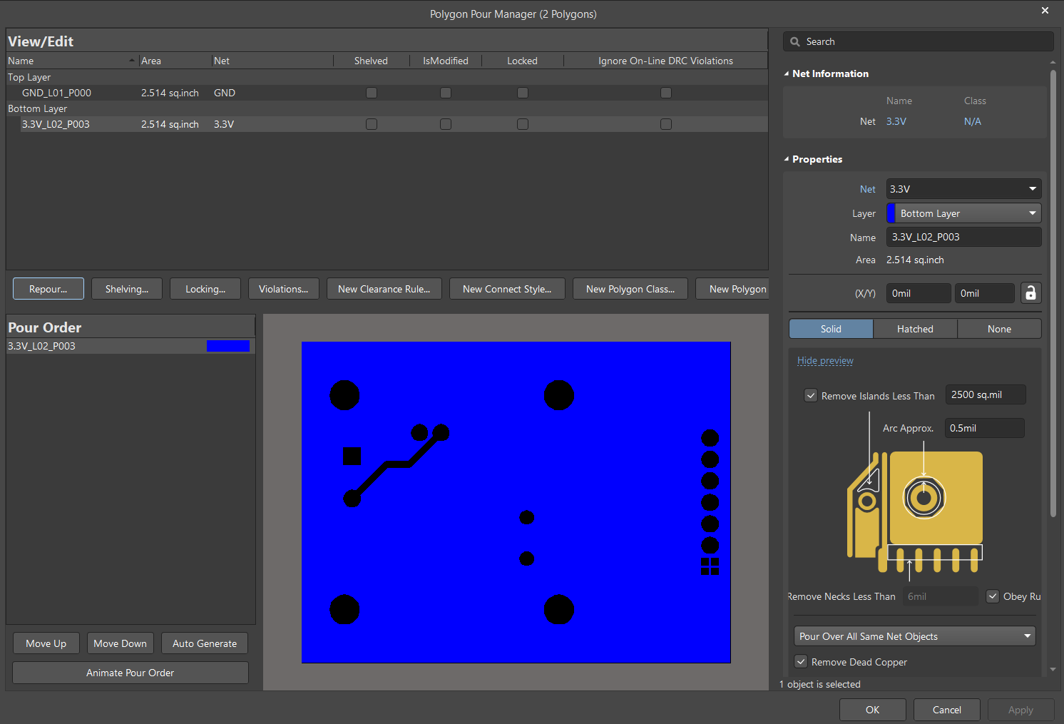
Here, a new window should open. You'll see a full view of each polygon you made without the components.
[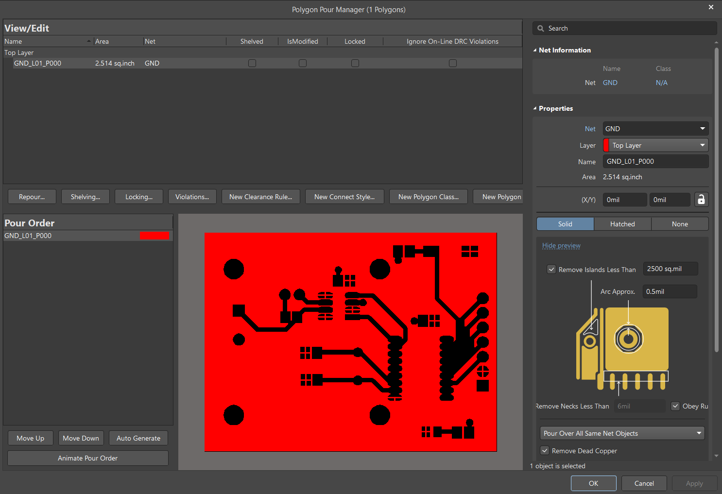](https://wiki.soonerrobotics.org/uploads/images/gallery/2026-10/3H8image.png)
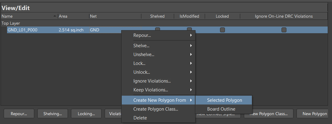
To create the second polygon, right-click on the Top Layer **GND\_L01\_P000** plane. Select **Create New Polygon From** --> then select **Selected Polygon**.
[](https://wiki.soonerrobotics.org/uploads/images/gallery/2026-10/9GKimage.png)
Now, this will create a copy of your polygon with the same net.
[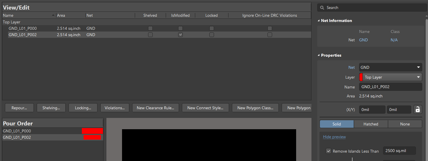](https://wiki.soonerrobotics.org/uploads/images/gallery/2026-10/RADimage.png)
With the second plane hightlighted, change the Net to **3.3V** and the Layer to **Bottom Layer**.
[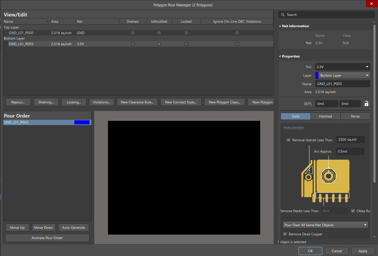](https://wiki.soonerrobotics.org/uploads/images/gallery/2026-10/lAqimage.png)
Once your plane's parameters are correct, select **Apply** on the bottom right of the window. A dialog box will pop up, select **OK**.
Your second polygon's view will now appear in the Polygon Manager, although not poured yet.
[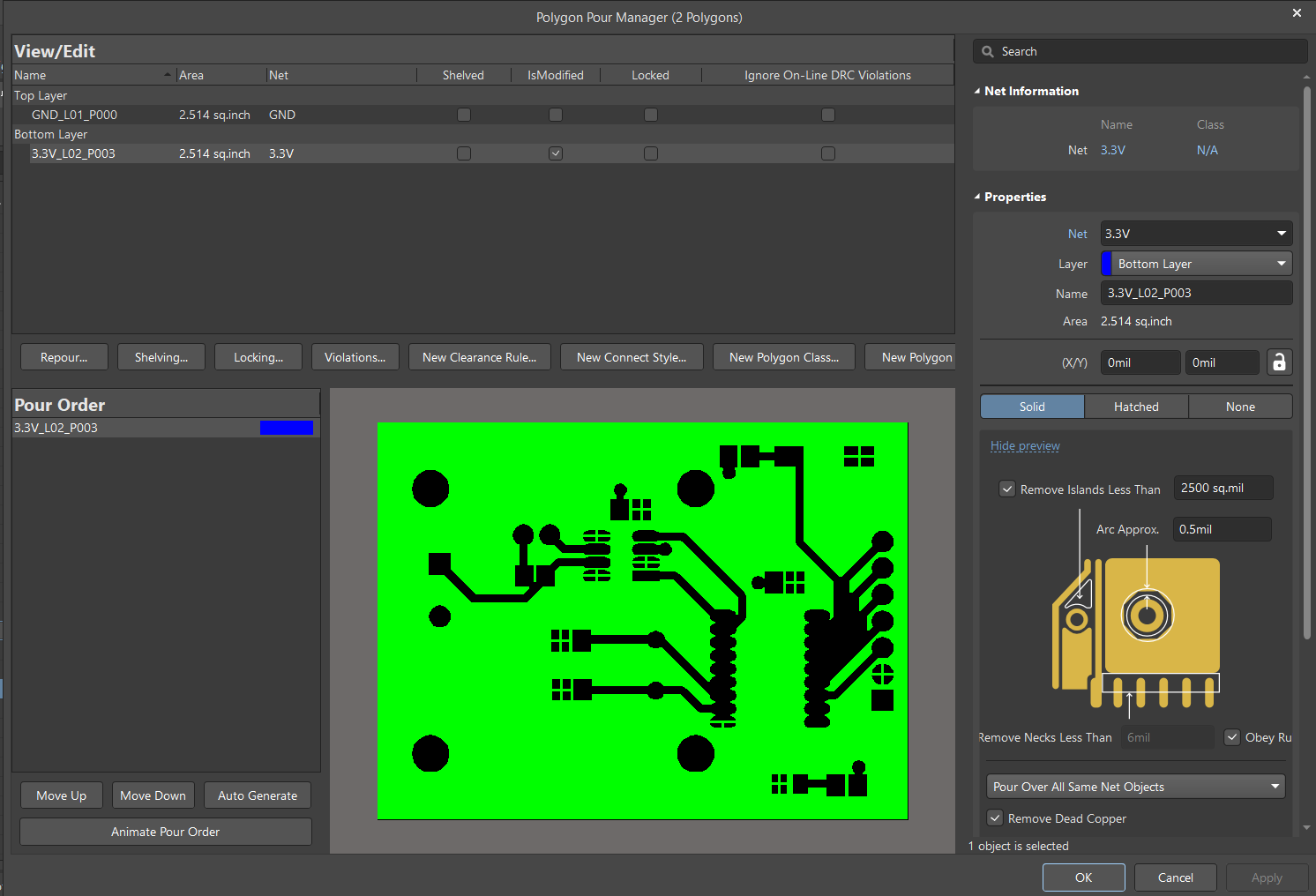](https://wiki.soonerrobotics.org/uploads/images/gallery/2026-10/HZbimage.png)
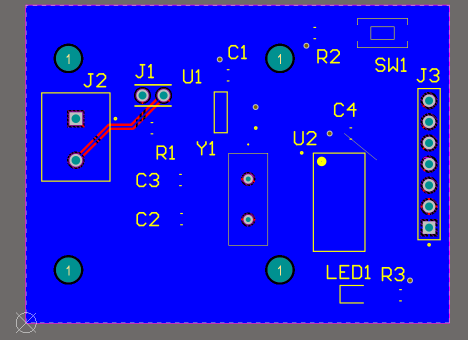
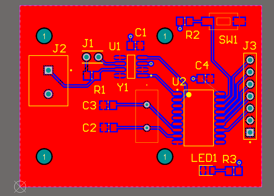
Next, select **Repour** on the left side of the window. Then select **Force Repour All Polygons**. Now, you have a newly poured 3.3V plane.
[](https://wiki.soonerrobotics.org/uploads/images/gallery/2026-10/c72image.png)
[](https://wiki.soonerrobotics.org/uploads/images/gallery/2026-10/G09image.png)
You can toggle between both planes to view traces on both sides of your board. Your board should now look like the following.
[](https://wiki.soonerrobotics.org/uploads/images/gallery/2026-10/UoDimage.png)
## Design Rule Check
The Design Rule Check is the next crucial step in ensuring your layout design fits the requirements set by your design rules.
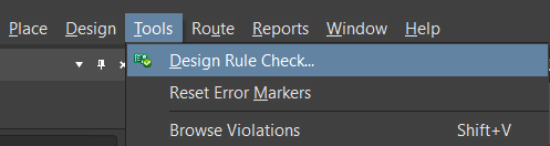
To run a Design Rule Check (DRC), navigate to **Tools**, then select **Design Rule Check**.
[](https://wiki.soonerrobotics.org/uploads/images/gallery/2026-10/2ckimage.png)
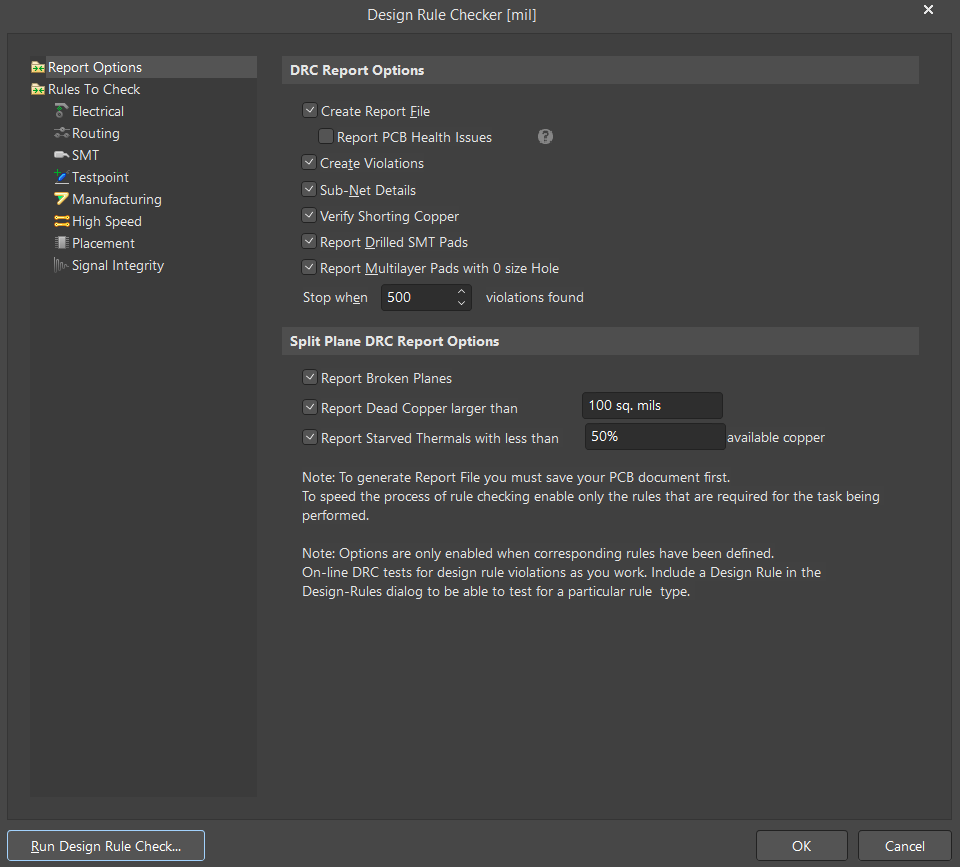
A new window will appear. Select **Run Design Rule Check**, then select **OK**.
[](https://wiki.soonerrobotics.org/uploads/images/gallery/2026-10/sYNimage.png)
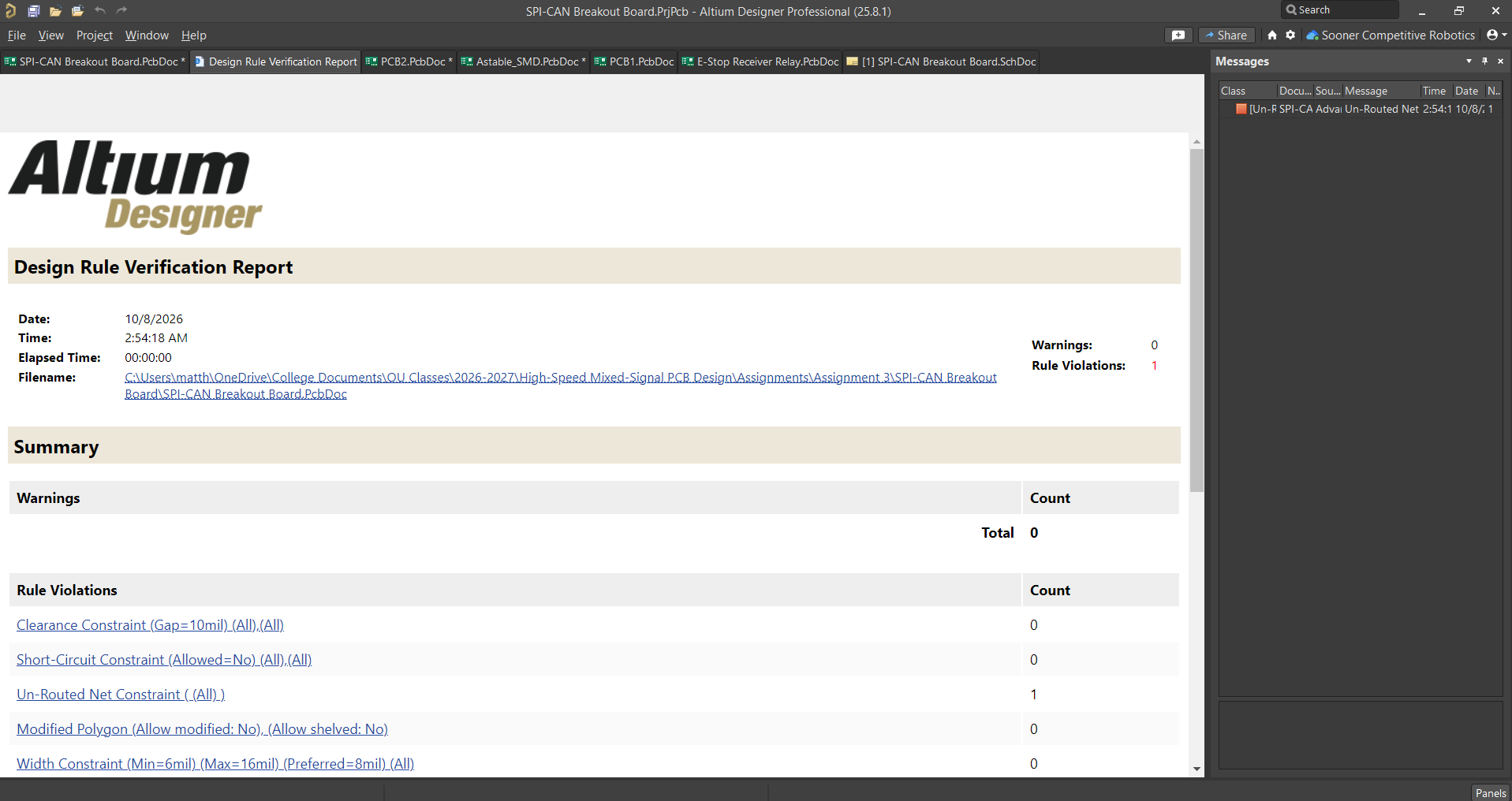
A new document window will open containing the DRC. As you can see, there's only 1 Rule Violation. This is really good!
[](https://wiki.soonerrobotics.org/uploads/images/gallery/2026-10/NuVimage.png)
The DRC will categorize each error by rule, so you may have multiple violations for a single rule. To check the rule violation, click the hyperlink called **Un-Routed Net Constraint (All)**.
[](https://wiki.soonerrobotics.org/uploads/images/gallery/2026-10/id9image.png)
Altium will take you down the page where the violation lives. Click on the hyperlink under the module.
[](https://wiki.soonerrobotics.org/uploads/images/gallery/2026-10/Gfhimage.png)
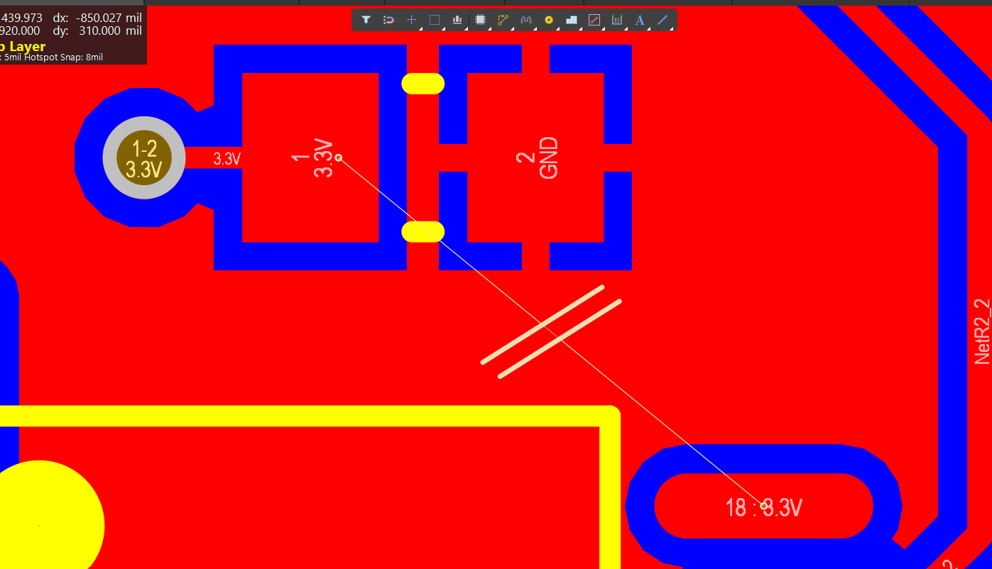
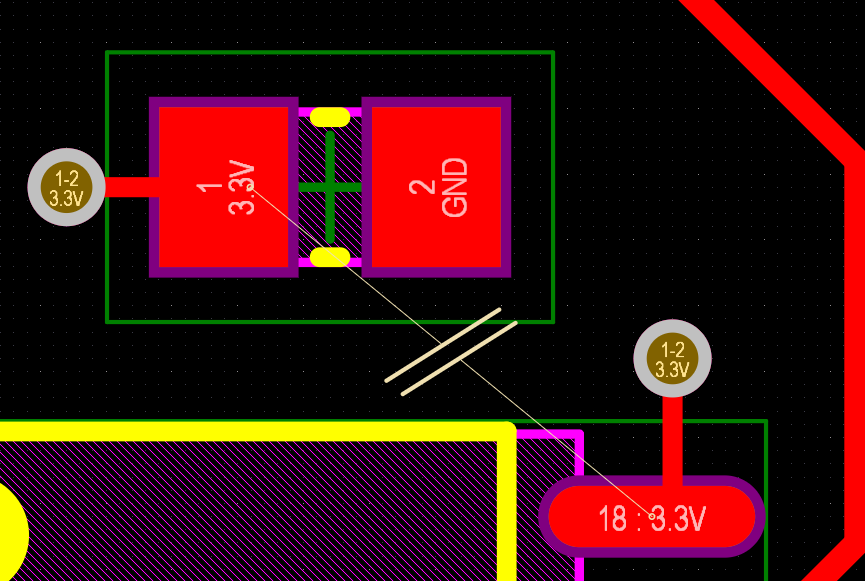
By selecting the hyperlink, you'll be taken back to your layout and shown where the error lives. In this case, there's no 3.3V signal routed to U2's 3.3V pad.
[](https://wiki.soonerrobotics.org/uploads/images/gallery/2026-10/Juximage.png)
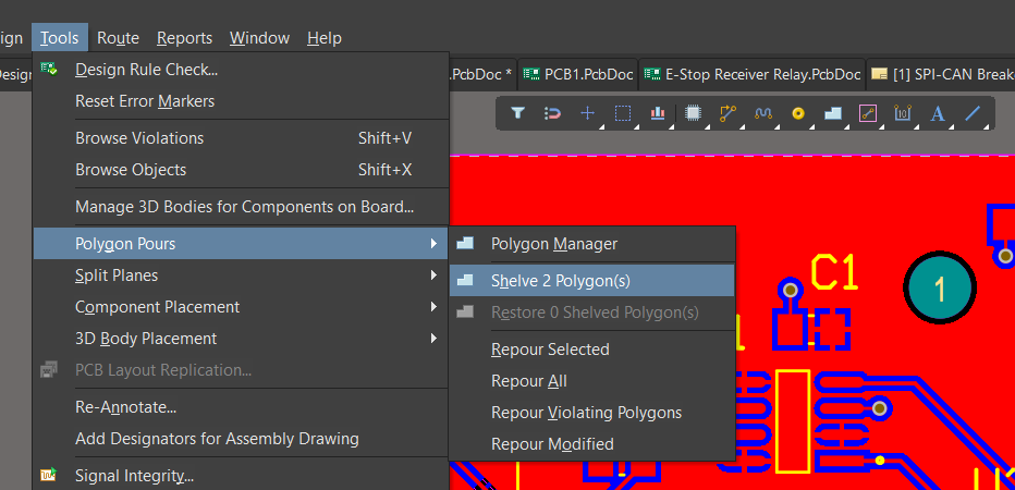
To fix this, go ahead and shelve your planes. You can do so by accessing **Tools** --> select **Polygon Pours** --> then select **Shelve 2 Polygons**.
[](https://wiki.soonerrobotics.org/uploads/images/gallery/2026-10/f00image.png)
With the polygons shelved, go ahead and attach a fanout via to U2's 3.3V pad.
[](https://wiki.soonerrobotics.org/uploads/images/gallery/2026-10/Svximage.png)
Once the error's fixed, you can run the DRC again. You'll find out that there are 0 rule violations! (or at least there should be...)
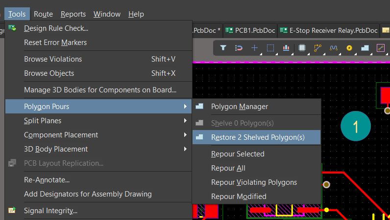
To return your planes, navigate to **Tools** --> select **Polygon Pours** --> then select **Restore 2 Shelved Polygon(s)**.
[](https://wiki.soonerrobotics.org/uploads/images/gallery/2026-10/rpEimage.png)
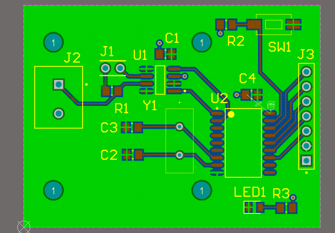
Altium will now return the polygon planes. As you can see from the green error markers, you'll need to repour your planes.
[](https://wiki.soonerrobotics.org/uploads/images/gallery/2026-10/sQVimage.png)
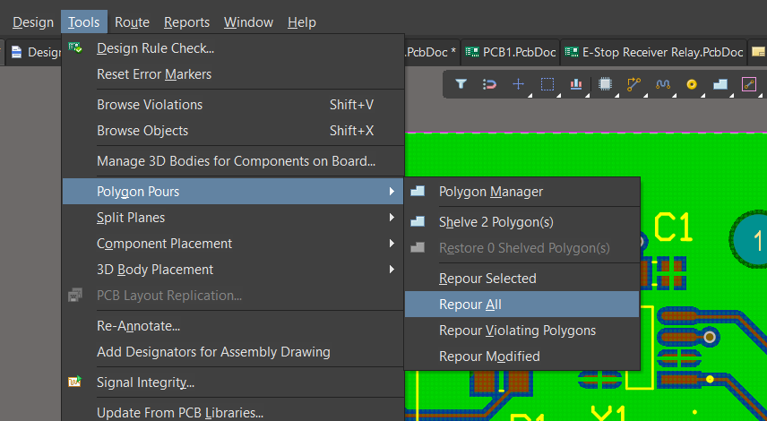
To repour your polygons, head to **Tools** --> select **Polygon Pours** --> then select **Repour All**.
[](https://wiki.soonerrobotics.org/uploads/images/gallery/2026-10/aOeimage.png)
With your polygons repoured, you should have a board similar to below.
[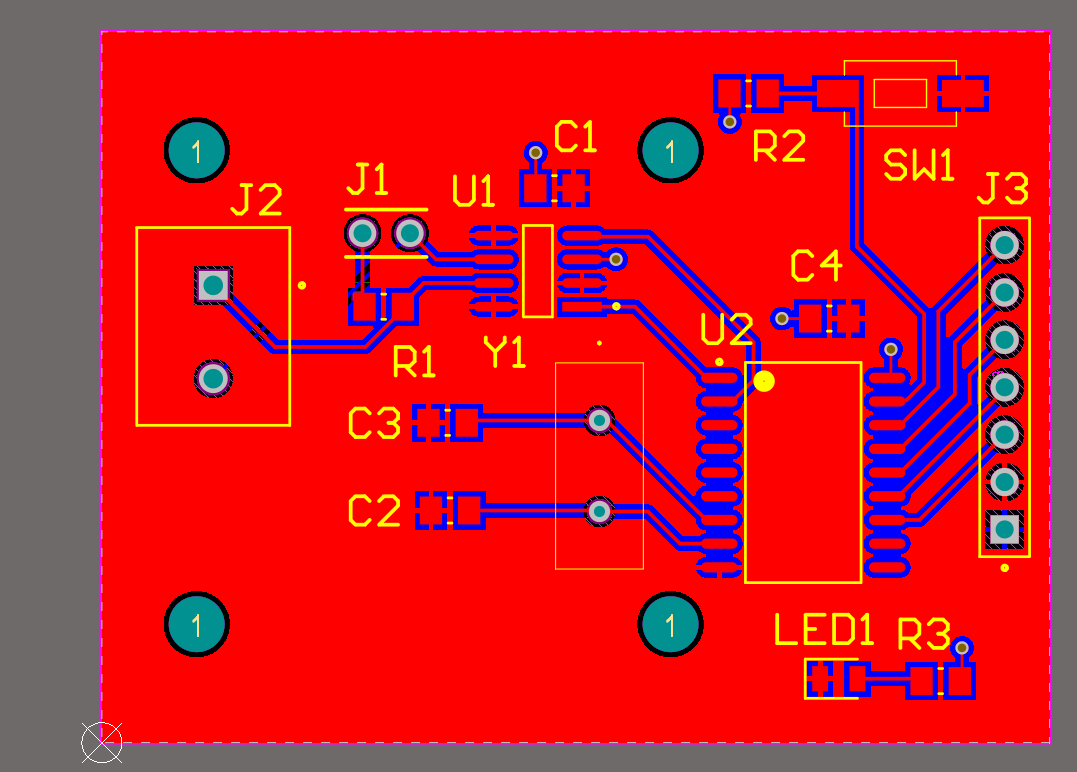](https://wiki.soonerrobotics.org/uploads/images/gallery/2026-10/STOimage.png)
## Board Customization
At this point, you'll need to add a personal touch to your layout and mark it as your own (and SCR's!)
Start by navigating to the top toolbar. Right-click on the "A" icon, then select **String**.
[](https://wiki.soonerrobotics.org/uploads/images/gallery/2026-10/8Bjimage.png)
Place this string on the outside of your board. You should see the red word String appear.
[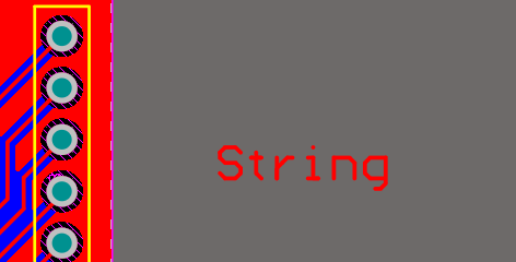](https://wiki.soonerrobotics.org/uploads/images/gallery/2026-10/r2fimage.png)
Go into the text's Properties window, and modify the string to state your name, and change the net to **Top Overlay**.
[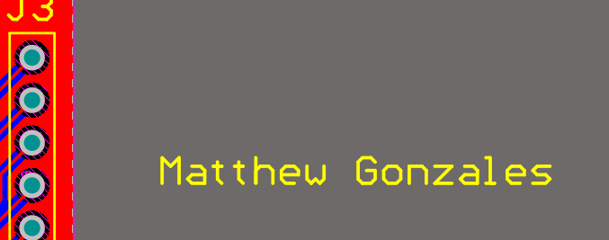](https://wiki.soonerrobotics.org/uploads/images/gallery/2026-10/NO1image.png)
Finally, move your name on to your board. From here, you can add the project name, component indicators, or even images on your board! (You can figure out that last bit).
[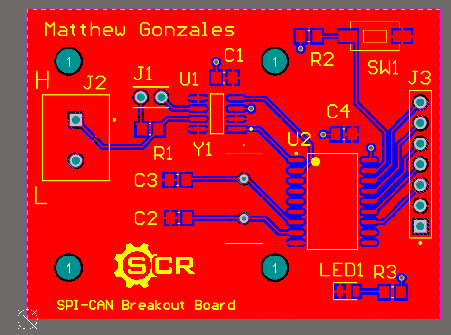](https://wiki.soonerrobotics.org/uploads/images/gallery/2026-10/duBimage.png)
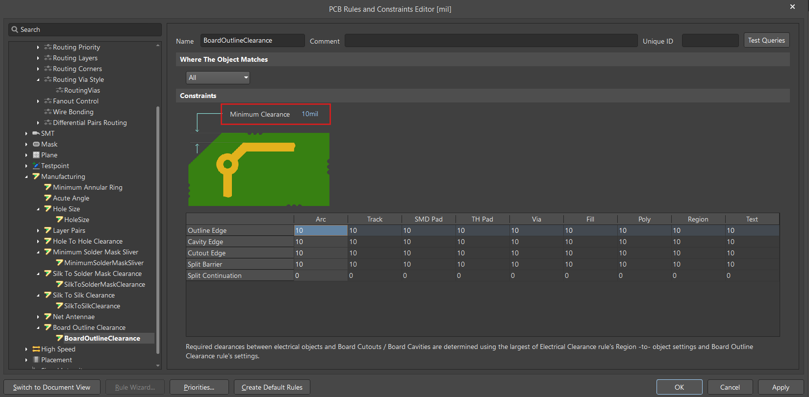
As a final step, you can add a trim around your board. When the board hits the manufacturer, part of the edge will be cut off.
To add this, update the Design Rules to include a new rule under **Board Outline Clearance**. Create a New Rule. Then, insert **10mil** into the Minimum Clearance.
[](https://wiki.soonerrobotics.org/uploads/images/gallery/2026-10/7IZimage.png)
Select **Apply**, and then **OK**. Repour your polygon planes. Now, you'll have a finished board layout with a trim.
[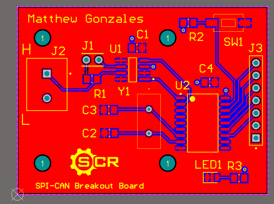](https://wiki.soonerrobotics.org/uploads/images/gallery/2026-10/XD7image.png)
To check the 3D view, select **View** on the top left tool-bar, then select **3D Layout Mode**.
[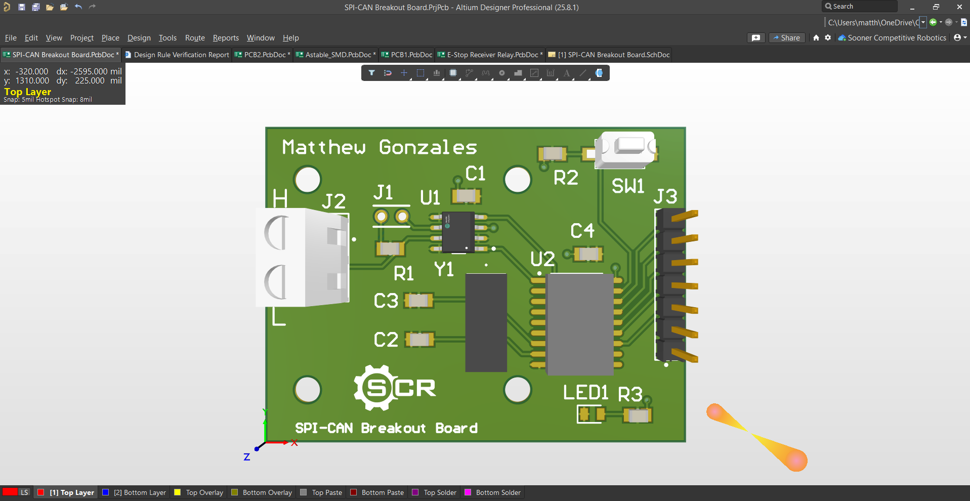](https://wiki.soonerrobotics.org/uploads/images/gallery/2026-10/21Eimage.png)
**Congratulations**! You just finished your first PCB!
Another section to this tutorial might be added later... but for now, enjoy your completed first project!