# PCB Development
# Producing PCB artifacts for JLCPCB
# Producing the artifacts
Guide for how to create PCB artifacts for ordering PCBs through JLCPCB
## 1. Run the DRC (Design Rule Checker)
In Altium, go to `Tools > Design Rule Check..`. In the pop-up window, click `Run Design Rule Check...`.
Verify that there are no *important* issues. For example, you can ignore violations regarding "Silk" (silk screen) and some clearance violations. This comes with practice to know which violations are or aren't important.
## 2. Create the artifacts
Follow the instructions for `Generating Gerber file` and `Generating NC Drill File` at [https://jlcpcb.com/help/article/8-How-to-export-Altium-PCB-to-gerber-files](https://jlcpcb.com/help/article/8-How-to-export-Altium-PCB-to-gerber-files)
> **Advanced Tip**
> You can customize your DRC to use rules that are specifically tuned for JLCPCB. Download the `RUL` (rules) file available on the above page. See [https://www.altium.com/documentation/altium-designer/defining-scoping-managing-pcb-design-rules#exporting-and-importing-rules](https://www.altium.com/documentation/altium-designer/defining-scoping-managing-pcb-design-rules#exporting-and-importing-rules) for instructions on how to import rules. Then, run the DRC again using the new rules which are optimized for JLCPCB.
## 3. Zip the artifacts
Once you have completed the steps above, you should see several new files under your Altium project, as seen below. Your files may differ depending on your project, but there should be some.
[](https://wiki.soonerrobotics.org/uploads/images/gallery/2025-08/altium-artifact-files.png)
Finally, we need to zip all the files. Right click any of the files and select `Explore`. This should open the folder all your files are contained inside. Navigate to the parent folder. Then, right click the folder with all your artifacts and zip it up, as seen below.
[](https://wiki.soonerrobotics.org/uploads/images/gallery/2025-08/zipping-altium-artifacts.png)
Congrats! You now have a zip file ready to be uploaded to JLCPCB and be ordered.
# Verifying the artifacts are correct
Verify your zip file will work by uploading it to the JLCPCB ordering page at https://cart.jlcpcb.com/quote (This is just to verify, you aren't actually going to order anything!)
Once you upload your zip file, JLCPCB will take a few seconds to process. After it is done, it should look like the screenshot below. Make sure it says `Detected X layer board of YxZ` at the top and that the values are correct. Also make sure the autopopulated values in the `Dimensions` field are correct.
[](https://wiki.soonerrobotics.org/uploads/images/gallery/2025-08/jlcpcb-confirmation.png)
Finally, click on the `Gerber Viewer` link below the PCB preview images. Here you can view exactly how the PCBs will be manufactured. Make sure the top and bottom layers look correct, your silk screen is correct, and the drill holes are actually holes.
# PCB Design Guide
# Introduction
This guide is not a “How to Use Altium” document. Instead, it focuses on layout design practices and considerations that go beyond what’s covered in the standard onboarding process. It assumes you’re already familiar with basic Altium navigation and PCB creation. If you’re new to PCB design or still learning how to use Altium, refer to the onboarding documentation.
The two-layer board design section is written with beginners in mind. It simplifies explanations and avoids deep technical reasoning to minimize confusion. In contrast, the four-layer board design section was written for those who have already completed at least one two-layer board in SCR. It provides more detailed insight into design choices and introduces advanced layout considerations / techniques. To avoid redundancy, many of the foundational concepts from the two-layer section are not repeated in the four-layer section. If you're designing a two-layer board that involves more advanced routing or layout strategies, the four-layer section may help in certain cases.
Before modifying any documents, change the project file name, schematic file names, and PCB file name to reflect the project you are working on. Generally, it should follow this format:
- EStop\_Relay.PrjPcb
- EStop\_Master.SchDoc
- EStop\_MCU.SchDoc
- And so on…
At the very least, capitalize the first letter.
**If changes need to be made to this document, contact the officer team.**# Schematic Formatting
Before placing any components or starting a design, modify the labels on each schematic document to reflect the project you are working on:
- Schematic properties such as name, team, PCB title, etc.
- Open the "Properties" tab and go to "Parameters" to change these.
- PCB title
- PCB description
### Master Sheet, Sheet Symbols and Ports
The master sheet is how you connect signals across different sheets. Every time a new sheet is added, you must generate the sheet symbol.
- To generate a new sheet symbol, right click anywhere in the master document, hover over "Sheet Actions" and select "Create Sheet Symbol from Sheet".
- Select the sheet(s) you want to add.
- Then, place the sheet(s) symbol anywhere you want it to be.
To connect signals across sheets, you use **ports**. These function the same as net labels, but must be added to your sheet symbol in the master document. If you end up having a signal that is in two separate locations on one sheet, but needs to connect to another sheet, use a Port to connect to the other sheet and use a Net Label to connect it within the same sheet.
- To add ports to your sheet symbol, right click the sheet symbol, hover over "Sheet Symbol Actions", and select "Synchronize Sheet Entries and Ports".
- Here, you must select the sheet symbols to add (or delete) and choose accordingly.
- Whenever you change the name of a port in a schematic that was already added, you must synchronize the sheet entry.
- The ports on each sheet are connected accordingly by wire.
When using net labels or ports, utilize snakecase and all capital letters to label your nets. Also, make your label descriptive enough so that others besides you know what it is.
- **Example:** If you have an encoder for a motor on the right side of a robot, label your encoder A and B nets/ports as “RIGHT\_ENCODER\_A” and “RIGHT\_ENCODER\_B”
This ensures the label is easy to read and is consistent throughout the design.
### Circuit and Component Labeling
Major circuitry and components should be labeled by either a technical name or product name. They should also be separated by space or lines from other circuits or components.
- **Example:** Raspberry Pi Pico is labeled in one of the schematic documents of the template.
- **Example:** If the design has a buck converter included, name the circuit "Buck Converter", not its literal product number.
Parts that require values (capacitors, resistors, etc) should have their values labeled as well.
[  ](https://wiki.soonerrobotics.org/uploads/images/gallery/2025-08/labeled-resistors.png)
**Labeled Resistors in Schematic**
### PCB Revision Notes
While we do have a version control system, it is suggested to use a notes box at the top corner of a schematic to document major changes.
- You can also just add one large one on the master schematic of your project if you only have a few schematic sheets.
### Differential Pairs
Differential pairs are two traces that carry equal and opposite signals—used for high-speed or noise-sensitive communication like USB or Ethernet.
[ 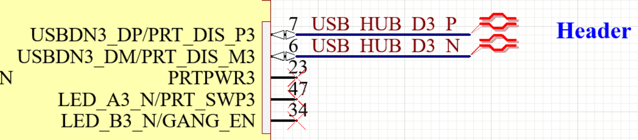 ](https://wiki.soonerrobotics.org/uploads/images/gallery/2025-08/scaled-1680-/differential-pairs-schematic.png)
**Differential Pairs in Schematic**
In Altium Designer, you define differential pairs by assigning nets a common prefix (like USB\_D+ and USB\_D-) and placing the differential pair designator on the net.
# Schematic Design Standards
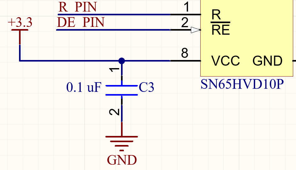
### Decoupling Capacitors
Every IC / microcontroller / voltage output should have at least one decoupling capacitor next to its power pin. The purpose of these is to filter out high frequency noise and ensure local voltage stability.
These are smaller (usually 0.1 uF), but check the datasheet to see if the manufacturer requires more than that value or more capacitors. These are usually 0805 capacitors, which are the generic capacitors in the Sooner Competitive Robotics part library.
[  ](https://wiki.soonerrobotics.org/uploads/images/gallery/2025-08/scaled-1680-/decoupling-capacitors-schematic)
**Decoupling Capacitors in Schematic**
### Bulk Capacitors
Bulk capacitors are similar to decoupling capacitors in that they should be placed close to the IC, microcontroller, or voltage regulator output—but they serve a different purpose. During sudden load changes, if there isn’t a nearby charge reservoir, the power supply may not respond quickly enough to maintain voltage, especially if the power trace is long or inductive. This can lead to a brownout, where the voltage drops drastically and may cause the microcontroller or other digital logic to reset, crash, or behave unpredictably. These capacitors are usually large (10 µF to 1000 µF), depending on how much current the system demands and how quickly that current may change. The 10 uF capacitors can come in the 0805 package, but larger values may require larger package sizes.
### Power Input Protection
Whether it is for a linear dropout regulator (LDO) or for a buck converter, a Schottky diode and transient voltage suppression diode (TVS) should be on the input.
The Schottky diode should be in series and the TVS diode should be in parallel. The TVS diode should come before the Schottky diode. Beginners should ask an experienced member about how to select these. Odds are, depending on the situation, that there are parts that are used across every board.
[  ](https://wiki.soonerrobotics.org/uploads/images/gallery/2025-08/scaled-1680-/power-input-protection)
**TVS Diode and Schottky Diode in Schematic**
### Test Points
Add a way to easily probe important or key signals.
- This can either be by headers or pad test points.
- Examples of "Key Signals": CAN lines and data lines for mission critical peripherals.
*Unfinished: Need walkthrough of how to do this.*
# Two Layer Board Design
### Two Layer Overview and Definitions
The two-layer PCB allows designers to route on the top and bottom layer. These are cheap, inexpensive, and will probably be the most common board stack-up used in SCR.
Below are a few definitions that will be useful when reading through the sections (and you should be familiar with):
- **Trace**
- A copper line that carries electricity (like a wire on the board).
- **Via**
- A tiny hole that connects the top and bottom of the board.
- **Pad**
- A metal spot where a component leg is soldered.
- **Net**
- A named connection between parts that should be electrically linked.
- **Plane**
- A big sheet of copper for ground or power.
- **Polygon Pour (Copper Pour)**
- A large filled-in area of copper, usually for ground.
- **Clearance**
- The space between traces to avoid shorts.
- **Track Width**
- How wide a trace is (wider = can carry more current).
- **Via Tent**
- A via covered with a solder mask to protect it.
- **Silkscreen**
- The printed labels/text on the PCB showing part names and outlines.
### Board Shape and Size
This is largely dependent on design, but most boards should resemble a rectangle or square and stay within 100mm x 100mm (3937.01 mil x 3937.01 mil). If the board becomes any larger than this, it ends up being more expensive. So, attempt to keep it within this range. If your board ends up being larger than this, make sure that you are utilizing board space adequately.
### Component Placement Considerations
When placing components on a PCB, start by positioning connectors like USB ports, power jacks, or headers where they need to be—usually along the edges or corners of the board. Next, group related components close together; for example, keep resistors near their associated LEDs or place capacitors right next to the microcontroller pins they support. Try to orient similar parts in the same direction to make the board neater and easier to work with.
Make sure not to cram components too tightly; leave enough space between them so you have room to route traces later. Decoupling capacitors, especially small ones like 0.1 µF, should be placed as close as possible to the power pins of integrated circuits to reduce electrical noise.
Don’t forget to leave space for mounting holes if your board will be screwed into a case or enclosure!
One way to organize your PCB is to think of each type of IC or circuit as a “city”. Place things that are alike close to other things that are alike and align them accordingly. For example, if you have two linear dropout regulators (LDO) that supply different voltage levels for your PCB, they should be relatively close in proximity to each other and have a similar layout in regards to their local capacitors.
[  ](https://wiki.soonerrobotics.org/uploads/images/gallery/2025-08/scaled-1680-/city-style-component-placement)
**"City"-Style Component Placement**
### Two Layer Routing Priority
When you begin routing your PCB, it is important to route things in order of importance to ensure short and direct traces for critical signals.
1. **Important fast signals (like clocks and USB)**
- Try to keep these traces short and on the top layer. Avoid holes (vias) that let the signal jump between layers because that can cause problems. If you need to, try to make the signal paths the same length so they arrive together.
2. **Signals with pairs (like USB 2.0 or SPI)**
- Keep these two wires close together and the same length. Run them on one layer over as much ground copper as possible to keep the signals clean. Try not to use vias here, and keep them away from noisy parts like power converters.
3. **Sensitive analog signals (from sensors or ADCs)**
- Keep these away from noisy digital parts and power lines. Use the shortest, most direct route and avoid vias if you can. Route these over ground areas to help keep noise out.
4. **Power**
- Use big areas of copper (polygon pours) for power and ground. If you have to use traces, make them wider so they can carry more current. Place small capacitors close to the IC pins to help smooth power.
5. **Digital control signals (like buttons or I2C)**
- Keep these signals grouped logically and make their traces short. Avoid crossing over sensitive analog areas.
6. **Low-speed signals (like LEDs or switches)**
- You can place these more flexibly. Use leftover space on the board, but don’t block important routes.
7. **Ground connections**
- If you must route ground traces, make them wide and connect the top and bottom ground areas with several vias. But it’s better to have large ground copper pours instead of thin traces.
### Two Layer Trace Width
Trace width is how wide the copper lines (traces) are on your PCB. Just like pipes, wider traces can carry more current. If a trace is too thin for the amount of current flowing through it, it can heat up, cause voltage drops, or even burn out.
Here are some simple starting suggestions:
- **Signal traces (like GPIO, I2C, SPI)**
- Use 0.25 mm (10 mils) – this is a common default and works for most low-power signals.
- **Power traces (under 0.5 A)**
- Use 0.5 mm (20 mils) or wider.
- **High-current traces (1 A or more)**
- Use 1 mm (40 mils) or more, or consider using a polygon pour instead of a trace.
- **Shorter = safer**
- Short traces can sometimes be a little narrower, but long ones should be wider to avoid resistance. If you’re ever unsure, it’s always okay to make your traces a little wider than needed—it adds safety and strength without much downside.
### Vias
Similar to copper traces, vias—the small plated holes that connect different layers of a PCB—need to be sized based on how much current will flow through them. Vias allow electrical signals or power to travel between layers, such as from the top layer to the bottom layer of a two-layer board.
For communication and low-power signals like GPIO, I²C, or SPI, only a tiny amount of current is used, so small vias are perfectly fine. A typical signal via might have a hole size of 0.3 mm (12 mils) and a pad size of around 0.6 mm (24 mils). These save space and work well for most digital signals.
However, for power lines or high-current paths, you need larger vias to handle the increased current without overheating or causing voltage drops. For example, a via carrying up to 0.5 amps might use a 0.4 mm hole with a 0.8 mm pad, while anything above that (up to a couple amps) may require 0.5 mm holes or more—and possibly multiple vias in parallel.
### Polygon Pours
Instead of drawing many thin traces for ground and power connections, you can just "pour" copper in unused areas and connect it to ground or power automatically. This helps keep the circuit more reliable and clean. Your bottom layer should have a ground pour that extends across the entirety of the PCB to ensure proper grounding. Once this is done, you can access the ground on the bottom layer by using a via and assigning it to the ground net. For power, depending on what voltages are present, you can place polygon pours to connect all of your peripherals accordingly. Polygon pours can be any kind of abstract shape, but try to make it as clean as possible and make sure that you are sufficiently connecting everything.
[  ](https://wiki.soonerrobotics.org/uploads/images/gallery/2025-08/scaled-1680-/polygon-pours-buck-converter)
**Polygon Pours Connecting a Buck Converter's Inputs and Outputs**
By default, Altium’s connection type for polygon pours is called a “spoke” connection or thermal relief. Whenever you connect a polygon to a net, each side that is exposed to it should have a spoke. If not, then rearrange the surrounding parts or resize the polygon to ensure proper connection. If you are unable to do this, then switch to routing that net with a regular trace.
[  ](https://wiki.soonerrobotics.org/uploads/images/gallery/2025-08/scaled-1680-/spoke-connection-polygon)
**Thermal Relief / "Spoke" Connection**
### Mounting Holes
For mounting holes, place a pad and make the hole size larger than the copper size.
[  ](https://wiki.soonerrobotics.org/uploads/images/gallery/2025-08/scaled-1680-/hole-size)
**Mounting Hole Configuration**
Bellow is a table showing some common metric screw sizes used by SCR and different "fits" for hole sizes. It is typically recommended to do the normal fit or loose fit for PCBs. M3 screws are the most commonly used screw for PCB mounting holes.
| Screw Size (M) | Nominal Dia (mm) | Close Fit (mm) | Normal Fit (mm) | Loose Fit (mm) |
| M1.6 | 1.6 | 1.7 | 1.8 | 2.0 |
| M2 | 2.0 | 2.2 | 2.4 | 2.6 |
| M2.5 | 2.5 | 2.7 | 2.9 | 3.1 |
| M3 | 3.0 | 3.2 | 3.4 | 3.6 |
| M4 | 4.0 | 4.3 | 4.5 | 4.8 |
| M5 | 5.0 | 5.3 | 5.5 | 5.8 |
**Metric Clearance Hole Sizes By Fit** # Four Layer Board Design
### Four Layer Overview and Definitions
Four layer PCBs offer many benefits over a two layer PCB, many of which will be discussed throughout this chapter. With a four layer board, the inner two layers can technically be whatever the designer chooses. But, for simplicity sake and to prevent issues, the four layer stack-up for SCR will be (top to bottom):
- Signal
- Ground
- Power
- Signal
[ 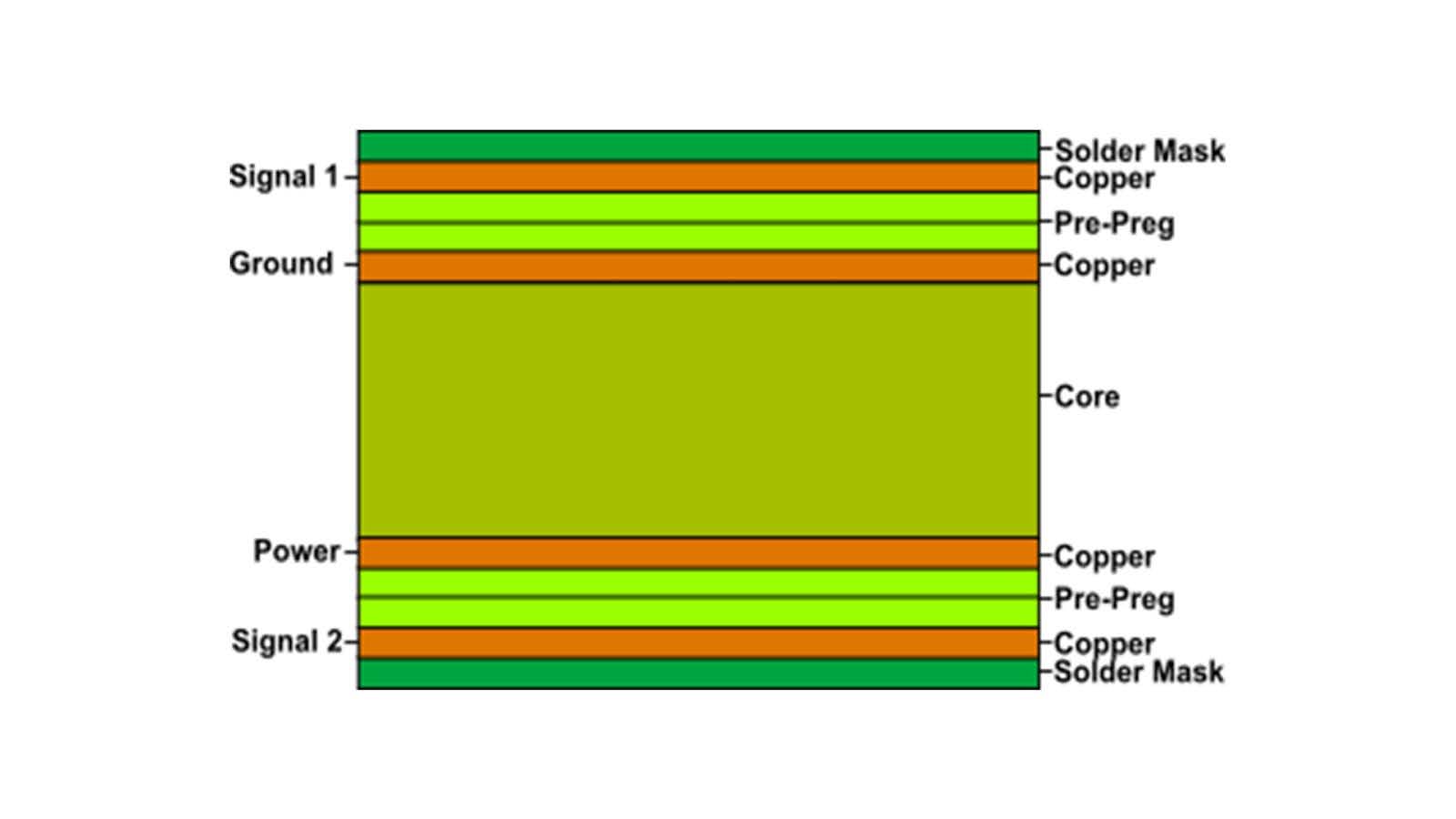 ](https://wiki.soonerrobotics.org/uploads/images/gallery/2025-08/scaled-1680-/four-layer-stackup)
**Four Layer Stack-Up Visualization**
Before discussing all of the considerations for routing a four layer board, some important definitions are needed for understanding why certain steps are taken:
- **Electromagnetic Interference (EMI)**
- Unwanted radiated or conducted energy emitted from a PCB that can interfere with other devices. Often caused by large current loops and improper plane usage.
- **Inductance**
- A property of traces or loops that resists changes in current. Higher inductance causes voltage spikes, noise, and EMI. It increases with trace length, loop area, and fewer ground returns.
- **Impedance**
- The total opposition a PCB trace presents to alternating current, combining resistance and reactance. In high-speed designs, traces act like transmission lines and must have controlled impedance.
- **Impedance Discontinuity**
- A sudden change in trace impedance due to a via, connector, pad, or change in trace width/layer, which causes signal reflections, degraded rise time, and ringing.
- **Current Loops**
- The closed path taken by return currents. Large loops increase loop inductance and can radiate EMI.
- **Tightly Coupled Signal-Return Pair**
- “Good Coupling”, controlled electromagnetic relationship between a signal and its return path (typically a solid GND plane), or between adjacent power and ground planes.
- **Parasitic Coupling**
- Unintended interaction between electrical signals due to their physical proximity on a PCB. It happens when energy from one trace ("aggressor") influences another nearby trace ("victim") through electric (capacitive coupling) or magnetic (inductive coupling) fields.
- **Reflection**
- Signal reflection occurs when a signal encounters a mismatch in impedance (e.g., at a via, connector, load, or trace discontinuity). Instead of being fully absorbed by the load, part of the signal bounces back toward the source. This can cause overshoot, undershoot, or signal distortion, especially in high-speed designs or long traces.
- **Reference Plane (Ground Plane)**
- The return path or plane a signal references. For proper signal integrity, all signals should have a clear, low-impedance ground return, typically a continuous internal GND plane on a 4-layer board.
- **Split Plane**
- Occurs when traces are routed on the ground or power planes. If a trace on the top or bottom layer crosses a gap between split power or ground planes, it can disrupt its return path. This forces the return current to detour, increasing EMI and signal distortion.
### Important Four Layer Rules
Four-layer PCBs offer significant advantages: they streamline routing, make it easier to manage signal integrity, provide clean return paths that minimize current loops, and make impedance matching far easier than on two-layer boards.
To preserve these benefits, ** traces should NEVER be routed on the dedicated ground or power plane layers. **
While a single small trace on a power plane might not cause catastrophic issues, routing multiple or critical signals on these layers introduces serious problems:
- Plane Splits
- Traces break the continuity of the plane, which eliminates the consistent return path underneath signals routed above it.
- Impedance Discontinuities
- Breaks in the reference plane can cause reflections, ringing, and degraded signal integrity.
- Increased EMI
- Larger return loops and poor containment of high-frequency energy result in higher electromagnetic emissions.
- Fallback to Two-Layer Habits
- Once the planes are compromised, routing ground or power on the outer layers will have to happen, effectively losing the advantages of the four-layer stackup.
Four layer boards are slightly more expensive than two layer boards at JLCPCB’s default size. But, once a four layer board becomes larger than this default size, the price quadruples. Because of this reason, you can make the board smaller than the one in the template, ** but you CAN NOT make the board larger than 100mm x 100mm. **
If you somehow need more space, you need to switch to a two layer board or discuss with a captain or officer about making a larger four layer board.
Two Layer Board, Smaller than 100mm x 100mm: $2.00
Four Layer Board, Smaller than 100mm x 100mm: $7.00
Two Layer Board, Larger than 100mm x 100mm: $9.70
Four Layer Board, Larger than 100mm x 100mm: $31.70
### Four Layer Routing Priority
When routing a PCB, it is important to know the order in which you should route each signal. The reason being that if you were to route a high-speed or sensitive signal last, you could end up having to pass between the top and bottom layers multiple times to get to an input or output or be forced to route near noisy signals. Doing this can lead to degraded signal integrity.
To avoid this, signals should be routed in this order:
1. **High-Speed/Timing-Critical Signals (clocks, crystal oscillators, USB 3.0, SPI (>10 MHz))**
- Route first on top layer over solid GND plane, try not to use vias or switch layers, match lengths if needed.
2. **Differential Pairs (USB 2.0, LVDS, SPI (<10 MHz))**
- Maintain spacing and equal lengths, route on the same layer over continuous ground plane, minimize the usage of vias, keep away from noise such as a buck converter output.
3. **CAN Bus**
4. **Sensitive Analog Signals (sensor inputs, ADC)**
- Isolate from digital and power, use short direct traces, avoid crossing noisy areas, minimize via usage, always over the GND plane.
5. **Power Traces**
- Use polygon pours where possible; if traces are needed, increase size for current; place decoupling caps close to pins; stitch vias to ensure low impedance connection with power plane.
6. **Digital Control/Comms Signals (e.g., GPIO, I2C)**
- Group logically, keep short and clean, avoid crossing sensitive areas.
7. **Low-Speed/Non-Critical Signals (e.g., LEDs, buttons)**
- Flexible placement, avoid blocking key paths, fill gaps in congested areas.
8. **Ground Traces (if needed)**
- Use wide, well-via-connected traces; solid planes preferred for return paths.
### Four Layer Trace Width
Trace width is usually dictated by the amount of current required to flow through the trace and how much the temperature is “allowed” to rise. Most signals can use the template default trace width and function just fine, as they have very low current requirements. For more power hungry signals, the IPC 2221 Trace Width Calculator can be used to find the required width.
*If you are needing to calculate trace width for a trace, you most likely should be using a polygon pour instead!*
However, in situations such as routing a signal trace to a surface mount pad that is significantly larger than the trace:
- It creates a vulnerable connection that could be easily broken or damaged during the soldering process.
- In some cases, it can result in a large impedance discontinuity that could cause signal integrity issues.
For this reason, it is suggested that the trace width is adjusted to match the pads better to prevent these issues, within reason.
If the trace has to increase significantly in width to connect to a pad, via, or pin, or is impedance matched, a teardrop connection would be a better option.
### Polygon Pours and Planes
In a 4-layer design, power integrity and signal integrity are highly dependent on how you manage your internal planes. The GND layer (Layer 2) should be treated as a continuous reference plane — do not split it. All high-speed or sensitive signals on the outer layers should be routed with a solid reference to this plane to minimize loop area and reduce EMI. This is especially important for differential pairs, clock lines, or any signals with fast edge rates. For power distribution, Layer 3 (PWR) should use solid polygon pours for each rail. If multiple voltages are needed, isolate the pours using keepouts or split regions, but avoid aggressive fracturing. Every power pour must have a clear and nearby return path to GND — this is why PWR sits directly adjacent to GND in this stack-up. Avoid routing signals in the power layer to maintain integrity and reduce noise injection.
[  ](https://wiki.soonerrobotics.org/uploads/images/gallery/2025-08/scaled-1680-/multiple-voltage-power-plane)
**Multiple Voltage Power Plane**
All polygon pours on signal layers (Layers 1 and 4) should default to GND, unless there's a specific reason to pour another net. In those cases, keep the pour away from sensitive routing and ensure it's well stitched with vias to the internal ground plane. Use thermal reliefs (spoke connections) for pads and vias to balance manufacturability with electrical performance.
Finally, make sure to stitch GND vias liberally between the outer layers and the internal ground plane — especially near signal vias, layer transitions, and around the board perimeter. This minimizes impedance discontinuities and forms a solid return path network.
### Polygon Pour Keep-Out Areas
There are cases where you do not want a polygon pour to fill a region. Common examples include:
- **High-speed signal escape zones**
- Under differential pairs or high-speed memory interfaces, where return paths may become fragmented or introduce stubs.
- **Analog sections**
- Noisy GND pour could couple digital switching noise into sensitive analog circuitry.
- **Crystals and oscillators**
- Local ground planes can sometimes do more harm than good due to parasitic capacitance and increased loop area.
- **Antennas or RF traces**
- Controlled impedance and radiation patterns could be distorted by surrounding copper.
In Altium, you can define keep-out areas specifically for polygon pours. Simply draw the region inside your pour, and it will be excluded. This works per-polygon, so if you have multiple pours over the same net, each one needs its own cutout.
### Teardrop Connection
Sometimes increasing trace width to better connect to a via or pad is not possible.
If this is the case, a teardrop connection can be used. A teardrop connection keeps the trace width the same, but gradually widens it as it connects to a via or pad. This helps with all of the issues outlined in the previous section, but also allows for connection of impedance matched traces. This gradual transition between the impedance matched width and the pin/via/pad reduces the impedance discontinuity.
For differential signals, it is suggested to refrain from using this type of connection, as it may cause issues due to the space between traces changing.
[ 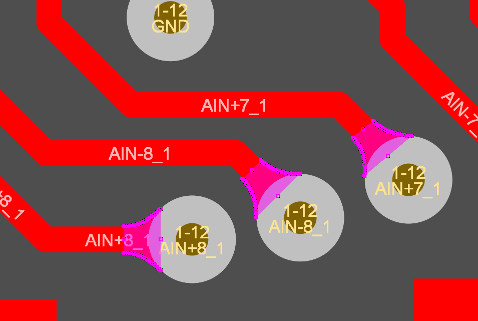 ](https://wiki.soonerrobotics.org/uploads/images/gallery/2025-08/scaled-1680-/teardrop-connection-type)
**Teardrop Connection Type**
### Signal Return Paths
A clean and low-impedance return path is crucial for signal integrity and EMI reduction. On a multilayer PCB, return currents typically flow in the nearest reference plane directly underneath the signal trace.
[  ](https://wiki.soonerrobotics.org/uploads/images/gallery/2025-08/scaled-1680-/signal-return-paths)
**Return Path Visualization**
For high-speed or sensitive signals, ensure that the signal trace runs over a continuous solid ground plane without gaps or splits. Interruptions in the ground plane force return currents to detour around voids, increasing loop area and causing unwanted noise and radiation.
When signals transition between layers through vias, provide nearby ground vias to maintain a continuous return path and minimize loop inductance. Multiple ground vias around high-speed signal vias help reduce impedance discontinuities.
Avoid routing signals over isolated copper islands or split planes, as these can break return current paths and degrade signal quality.
By maintaining well-planned return paths, you reduce crosstalk, improve EMC performance, and enhance overall board reliability.
### Impedance Matching
Impedance matching ensures that a signal trace's impedance closely matches that of the source and load, which is typically 50 Ω for single-ended and 100 Ω for differential pairs. This becomes critical for high-speed signals (e.g., clocks, USB, SPI, and fast parallel buses), where mismatches can cause reflections, degraded signal integrity, or outright communication failures.
In a 4-layer stackup like SIG/GND/PWR/SIG, maintain controlled impedance by routing high-speed signals on the outer layers directly over the adjacent ground plane. The trace width, the dielectric thickness between layers, and the trace's distance to its reference plane all affect the impedance. Routing over power planes should be avoided for impedance-sensitive signals unless the power plane is well-decoupled and quiet—use ground as the primary reference.
You can calculate trace dimensions for controlled impedance using Altium's Layer Stack Manager and Impedance Profile tools. For an external check or second opinion, **Saturn PCB Design** Toolkit is widely used to perform quick impedance and stackup calculations. While it doesn't replace a professional fabricator’s tools, it's often close enough for practical design decisions. Ask for help from alumni or older members to verify calculations.
Focus impedance control efforts on critical nets, as not every signal needs matching.
### Differential Pairs
When routing:
- Keep the pair tightly coupled—constant spacing is more important than exact length, though both matter.
- Avoid stubs, via mismatches, or diverging paths; mirror bends if possible.
- Minimize layer transitions, but if needed, match vias on both traces and ensure return path continuity.
- Always route over a solid ground plane (Layer 2 in your SIG/GND/PWR/SIG stack) to maintain consistent impedance and a continuous return path.
### Via Stitching and Shielding
Via stitching involves placing multiple vias to connect copper pours (usually ground) between layers, improving return paths, shielding, and EMI performance. In a 4-layer board, stitching your ground pours together across layers (e.g., Layer 1 SIG to Layer 2 GND, or Layer 4 SIG to Layer 2 GND) ensures a low-impedance path for high-frequency return currents and minimizes loop area.
Use via stitching around high-speed traces and differential pairs. This helps shield signals from external noise and reduce radiation.
Stitch your power pours to the power plane with multiple vias near decoupling capacitors and ICs to reduce inductance and maintain low impedance across the power distribution network. This improves transient response and helps suppress power plane noise.
Careful via stitching strengthens the physical and electrical integrity of your multilayer design.
### Unique Situations
Here are some unique situations that did not have a section:
- N/A
# Design Validation
### Trace Validation
- **Power Trace:** Make sure it is the correct width or change it to a copper pour.
- **Signal Trace:** Make sure it is as short and concise as possible.
- **High-Speed Impedance Matched Trace:** Double check and make sure that the impedance of the trace is correct. Also, make sure noisy signals are as far away from it as possible (i.e buck converter outputs, other high-speed traces, etc).
- **Differential Pair:** Double check that the impedances are correct, the spacing between the traces is correct, and that the lengths of both of the traces are within tolerance for the signal.
- The length matching portion of this and the tolerance for it differs between signal to signal. Something like USB 2.0 is not as sensitive as something like DDR5 RAM (not that you would do DDR5 routing in SCR). Double check the tolerances.
### Polygon Pour Validation
- Make sure that where there are polygon pours connecting parts together that they allow multiple connections to the pad and/or via.
- **Example:** If you are using polygon pours to connect a pad to a net, there should be three "spokes" connected to that pad (usually on all sides except one).
- If there is a dense area of parts connected to the same net with traces, consider swapping the traces out for polygon pours.
- Make sure to remove dead copper for any polygon pours, which can be done in the Polygon Manager.
- Large unconnected copper pours can be a source of EMI.
- **Mainly for Four-Layer:** Make a ground pour on the top and bottom layer, if you haven't already.
### Ground and Power Plane Validation
- Verify that **zero traces** split the ground plane.
- They shouldn't split the power plane either, but should **never** split the ground plane.
- If you have a mixture of voltages coming from different kinds of regulators on the power plane (i.e 3.3V from an LDO, 7V from a buck converter), make sure they are sufficiently spaced between each other.
- An LDO has a very clean output voltage, which is useful for supplying power to things like microcontrollers. Depending on the buck converter's switching frequency, it can be parasitic to an LDO's output.
### Adding Your Name and Graphics
Make sure to add:
- Designed by: *Your Name*
- SCR Logo
- This can be found on the SCR website
- Memes
- Make it your own! :)
When you add these graphics, make sure it is on the *Bottom Overlay* or *Top Overlay*. If you add it to one of the layers, it gets created out of copper, which is bad. If you decide to add something to the *Bottom Overlay*, you will have to mirror the image for it to print correctly.
- Press *Ctrl + F* to flip the board to see the bottom of the PCB.
# Generating PCB Outputs
### Output Job File
### Verifying Gerber and Drill Files on JLCPCB
# Reference Material
### General Reading Material
[Altium Designer: PCB Design Documentation](https://www.altium.com/documentation/altium-designer)
### Youtube
- [Phil’s Lab](https://www.youtube.com/@PhilsLab)
- Videos are usually under 30 minutes. Pretty beginner friendly.
- [Robert Feranec](https://www.youtube.com/RobertFeranec)
- Has some shorter form videos, but the majority span an hour or more. Some videos are not beginner friendly, outside of his general tutorial videos. But, if you want to learn higher level board design that SCR will most likely never have to do or learn the finer details of board design, he’s a great option.
- [Altium Academy](https://www.youtube.com/AltiumAcademy)
- The official Altium Youtube page. The videos are alright, but they are pretty short and can be informational.
### Saturn PCB Toolkit
- This software is only really needed if you are going to need to do impedance matching or higher level design, but it is a good tool to get familiar with.
- [Link to Software](https://saturnpcb.com/saturn-pcb-toolkit/)
# Document Revision Notes
06/07/2025: Created the document, created and updated sections with starting info (B. White, Rev 0.1)
07/23/2025: Reformatted document to include two-layer board design as well (B. White, Rev 0.5)
08/01/2025: Migrated guide to new SCR wiki (B. White, Rev 0.5)
# Introduction to Altium Designer