
Electrical
Overview
Welcome to electrical onboarding for the 2025-2026 school year!
Goals
- Learning
- What is a PCB (Printed Circuit Board)?
- What is a Schematic?
- How do you read a Schematic?
- Practical
- Soldering components on a PCB
- Debugging/Testing a PCB
Reading a Schematic
You can find the schematic for the PCB you will be working on here. The first three pages contain the actual schematic for the PCB, although you can mainly ignore the first page as it is purely for connections across sheets. A schematic is just a logical and visual representation of the PCB. The third (last) page of the pdf contains a top down view of the board with all of its layers.
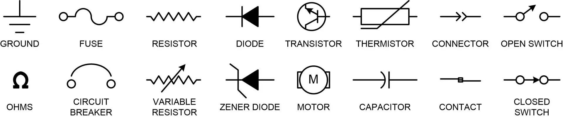
The schematic is full of like some of the ones seen below.
voidYou hello_world()may {also }noticed


Components & Symbol
Throughout the schematic
Soldering Basics
PCB Assembly
Testing
| Designator | Part | Notes |
|---|---|---|
| Header | Title | |
| Paragraph | Text |