
2. Creating a Schematic
Introduction
Creating a schematic in Altium is one of the most important steps in PCB Design. Before you create a schematic from scratch, you should already have a good idea about what your PCB will be used for, the logic behind the design, and critical components that will allow for successful operation.
During the schematic design process, you'll typically follow these steps:
- Requirements - Deciding the necessary interfaces, constraints, etc.
- Project Libraries - Determining which components are needed for your design.
- Component Arrangement - Organizing and wiring the components on your sheet.
- ERC / Compiling - Checking for errors and validating your schematic
Note: It's HIGHLY recommended to use a computer mouse when going through this tutorial.
Schematic Sheet Set-Up
When you start, you should already have a blank schematic loaded.
- For information on how to create a blank schematic, refer to 1. Project Creation
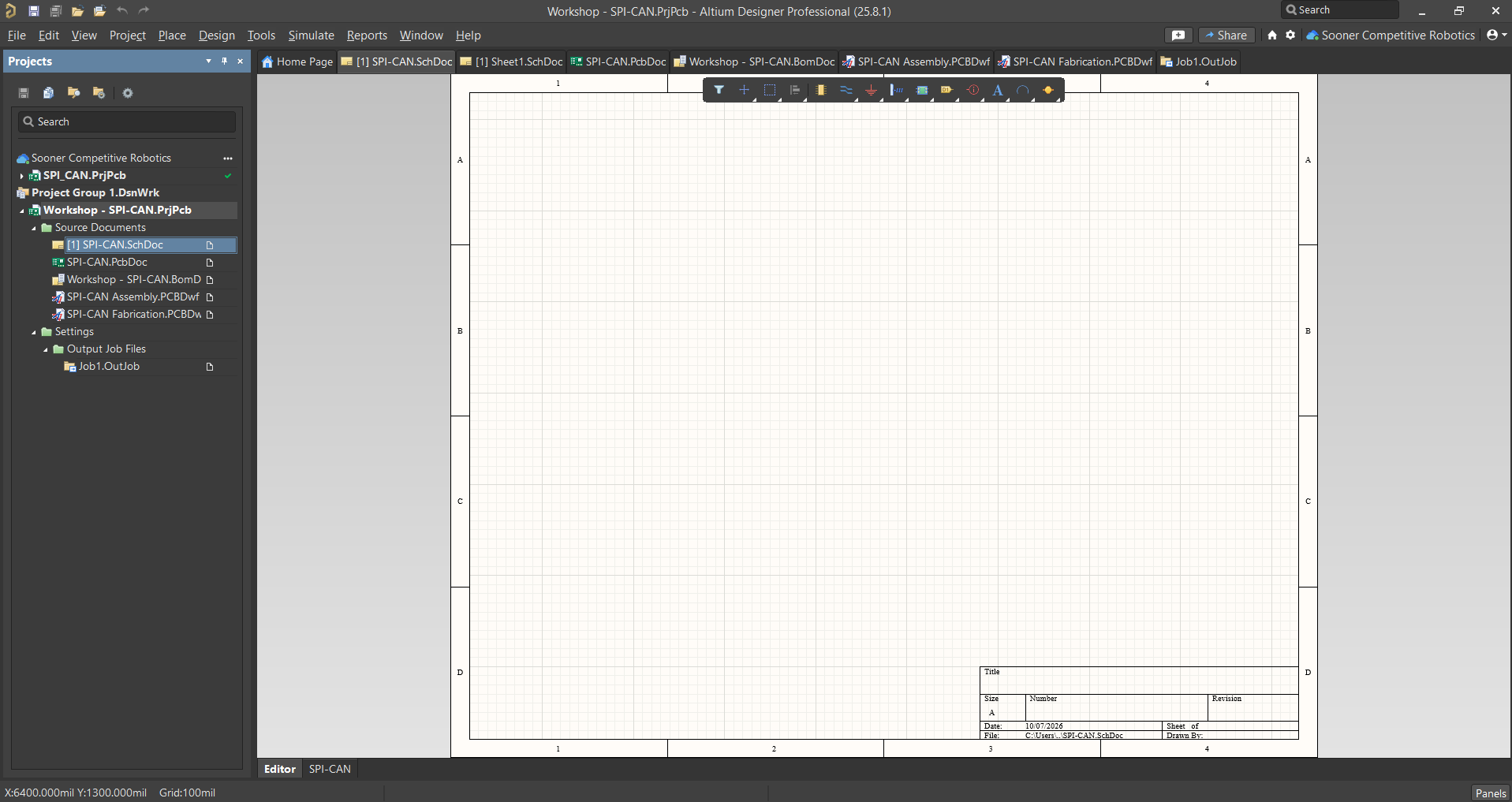
As you're creating your schematic, it's helpful to know these controls:
- Right-Click & Hold: Moves the Page
- Scroll Wheel: Move up and down on the Page
- Ctrl + Scoll Wheel: Zooms in-and-out of the Page
Before designing your circuit schematic, it's important to make sure your sheet has everything set-up properly. This includes the Sheet size, title, author, and more.
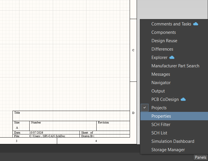
A new window should appear as seen below:
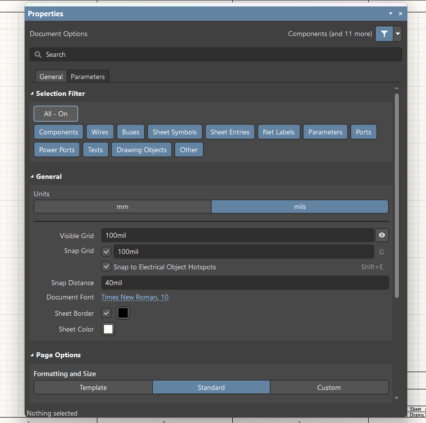
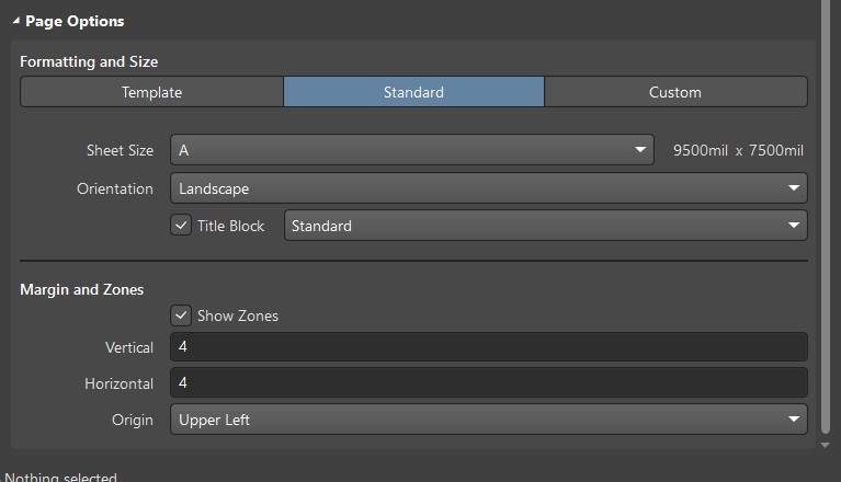
If you scroll down, you can modify the Sheet Size, Orientation, and more! For now, we'll leave the settings as they are.
If you select the Parameters tab (under the Search Bar), you can modify the sheet's elements.
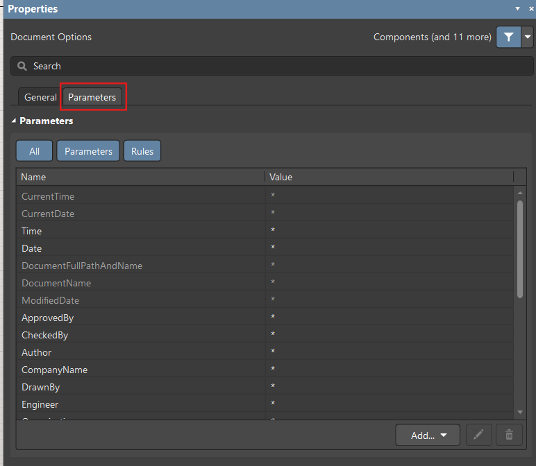
Go ahead and modify the following parameters with the following values:
- Date - Today's Date
- Author - Your Name
- Title - "SPI-CAN Breakout Board"
- DocumentNumber - 1
- Revision - 1
Next, you'll need to place these values on the sheet. With the values set, exit out of the properties window and navigate to the top of the window.
You'll find a tool-bar filled with various icons. Hover over the "A" icon and right-click until a drop-down appears. Then, select Text String.
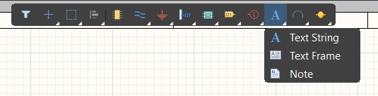
You'll see the word "Text" appear and move along with your cursor. To place it on your schematic, simply left-click on the sheet.

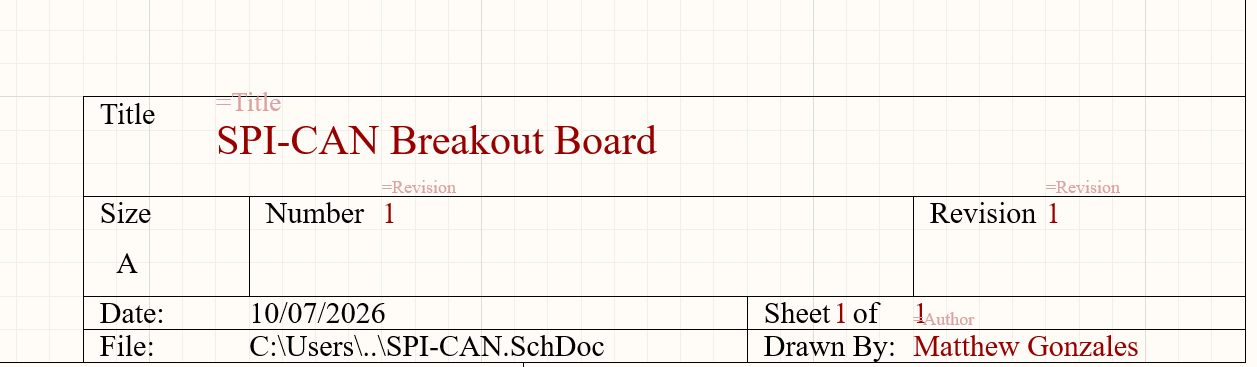
Like all objects placed on a schematic, you can left-click and hold down on an object to move it around. With this in mind, place a bunch of text boxes in the title block as arranged below:
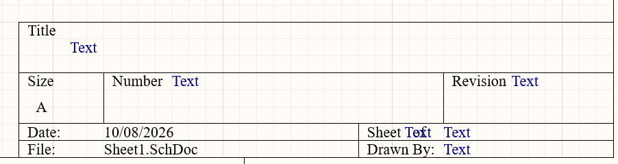
To update the text, right-click on a Text box, then select Properties
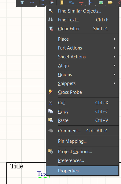
Next, in the drop-down arrow in the Text box, navigate to the value you want to attribute to your text box.
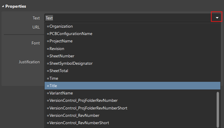
Go ahead and update the text boxes using the procedure above. You can also update the text size and color to your liking.
Component Selection & Placement:
You're now ready to begin placing components on your board. Typically, you'll need to conduct proper research on your circuit design beforehand. Fortunately, we have a design ready for you!
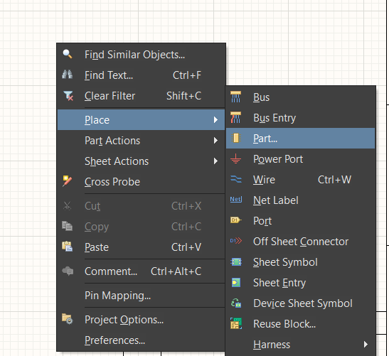
Start by right-clicking anywhere on the schematic. Then, select Place --> select Part.
A new window should appear, allowing you to search for parts from the Sooner Competitive Robotics workspace components library. To start, go ahead and insert the text "MCP2515-E/SO" into the Search box.
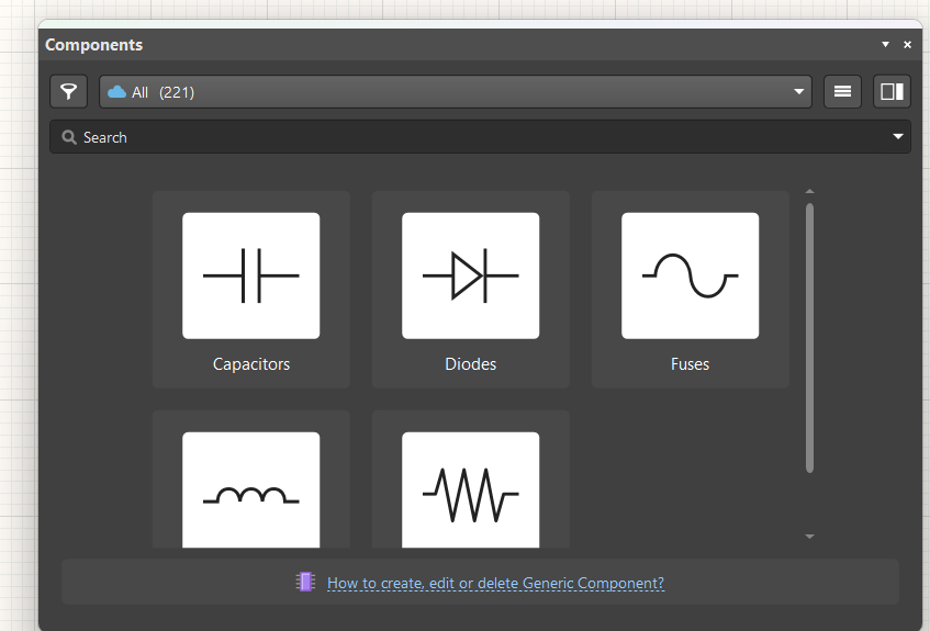
You should see the part you searched up appear below. If your desired component is not saved to SCR's custom parts library, you can always search for parts in the Manufacturer Part Search.
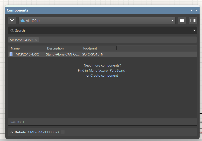
To place your part, double left-click the part's icon. A faded version of your part should appear on your schematic. Left-click on the sheet to place your part. Press esc on your keyboard to exit out of part placement.
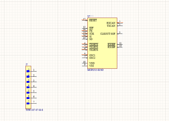
Once you exit out of the Components window, your part should appear on the page like below:
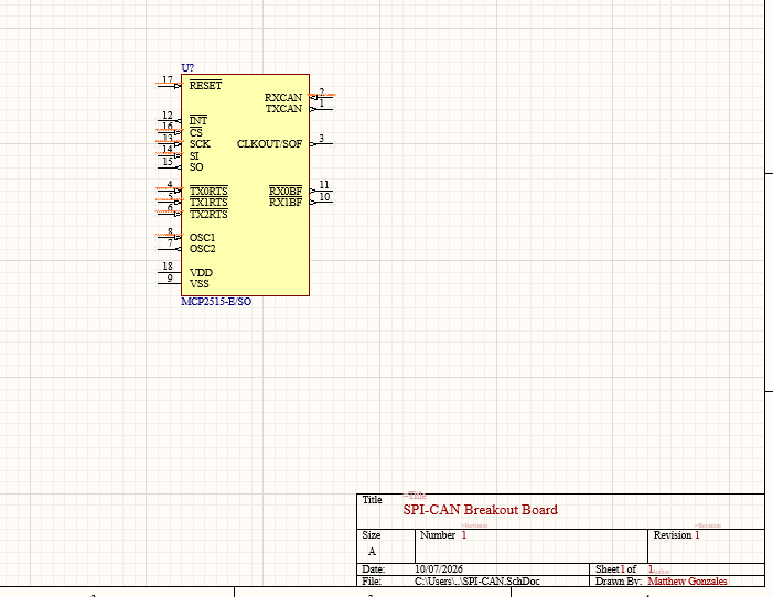
For one of the components, we'll need to access the Manufacturer Part Search. Open the Components window, then search up the part number "TSW-107-07-G-S." You'll notice this part doesn't appear in the search results since it's not stored in the SCR components library.
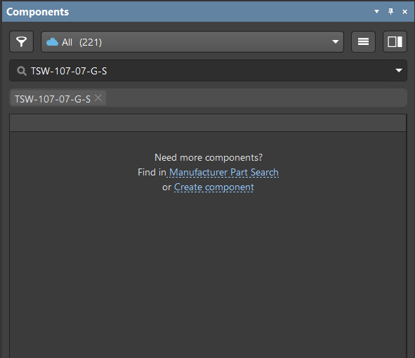
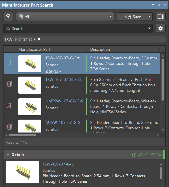
You can expand the SPNs tab. This will display the vendors that are currently selling the component.
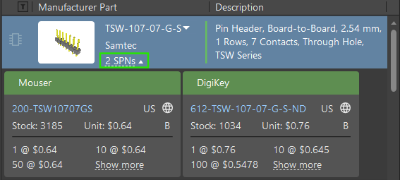
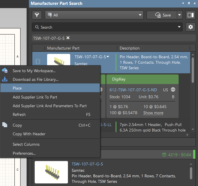
We'll go ahead and place the component from the top search result. To do so, right-click on the TSW-107-07-G-S, then select Place.
Place down your part. Your schematic should look like below.
Now, go ahead and place the required parts for your project using the procedure you just learned. A list of the required parts can be found below:
Note: for the capacitors and resistors, you're going to search up the string in bold. After placing the component, you'll modify the part's properties with it's required values. Info on how to do this is after the component list.
- 1x MCP2515-E/SO
- 1x MAX3051ESA+
- 1x LFXTAL057135Bulk
- 1x 2x1 Header
- 1x TSW-107-07-G-S
- 1x 2x1 screw terminal
- 1x AP2012SGD3
- 1x 6mmx3.5mm SMD Switch
- GENERIC CAPACITOR 0805 or 0603(1608):
- 2x 18pF
- 2x 0.1uF
- 0805 RES:
- 1x 120Ω
- 1x 220Ω
- 1x 10KΩ
- 1x 120Ω
Whenever you place down a capacitor, resistor, or any component with a custom value, you'll need to showcase the value on the schematic. When you place a capacitor, you'll see something like this:
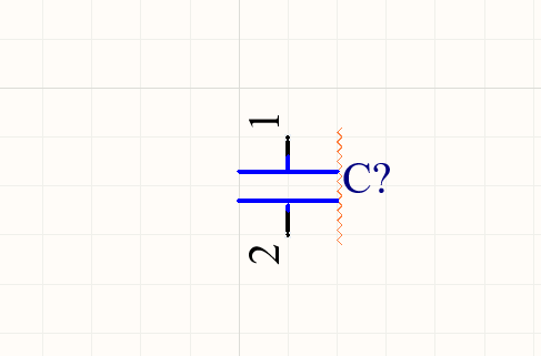
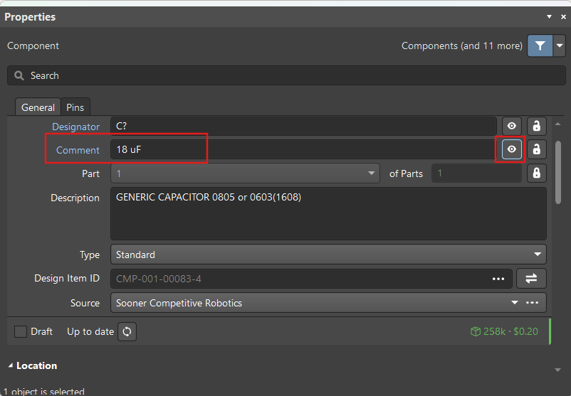
To assign the capacitor's value, double left-click on the newly placed component. Next, type in the capacitor's value into the Comment text box. Afterward, make sure the "eye" icon is enabled before closing out of your window.
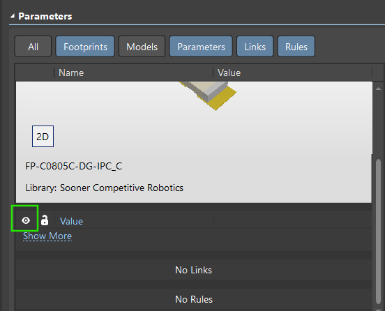
Then, scroll down to parameters and disable the eye icon for the Values parameter.
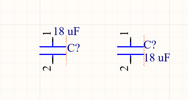
Your component should look like the capacitor on the left. You can move around the text surrounding the capacitor to make it more organized.
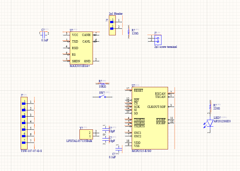
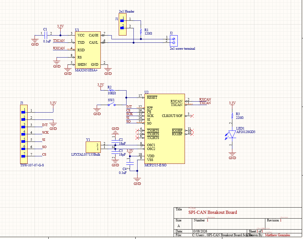
You can follow the same process for your resistors. When you're finished placing components, your schematic should look like the following:
Power Ports:
Next, you'll to place your Power and Ground references. These are necessary to understand how power flows through your circuit.
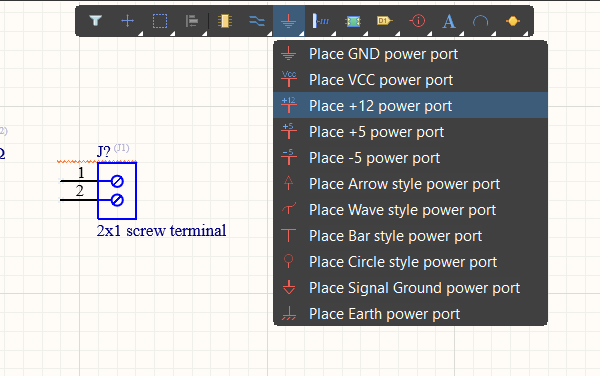
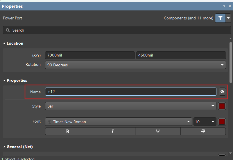
Once you place your power port, you'll need to update the value to +3.3 V. Double-click on the port you just placed and change the name from +12 to 3.3V.
Now, go ahead and place a GND port. When you're done, you should have two ports placed as seen below:
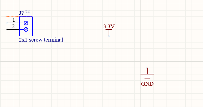
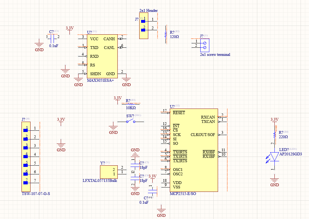
Go ahead and arrange the ports to their appropriate locations as seen below. Copy and Paste each port until you have:
- 10x GND Ports
- 5x 3.3V Ports
Note: While placing a component, you can press Space to rotate your part 90 degrees!
Component Wiring:
With your components laid out, we can go ahead and mark off any ports we're not using for our design.
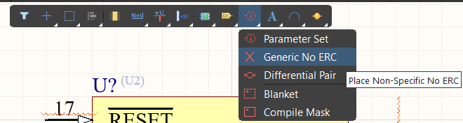
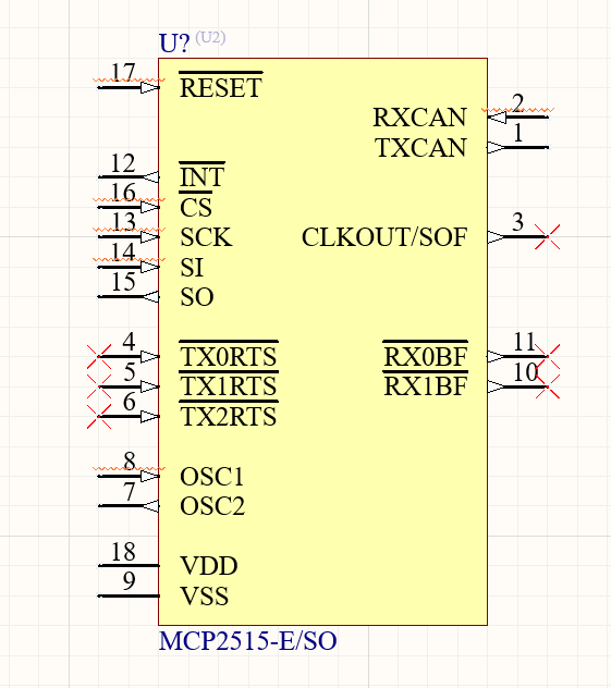
Then, go ahead and mark the following pins on the MCP2515-E/SO with the no connection indicator:
- TX0RTS
- TX1TS
- TX2RTS
- CLKOUT/SOF
- RX0BF
- RX1BF
Now, you can start wiring your components together. To enable the wire toggle, there's a couple of ways to do this.
- You can do the same thing by selecting Ctrl + W on your keyboard.
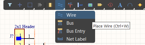
On your sheet, you should now see a faded cross-hair moving with your cursor. Wherever you left-click on the sheet, a wire will form.
Let's connect the 3.3V power port to the 2x1 Header. With the wire toggle enabled, left-click on the "1" port and drag your invisible wire to the 3.3V port. Left-click on the 3.3V port to connect your wire.
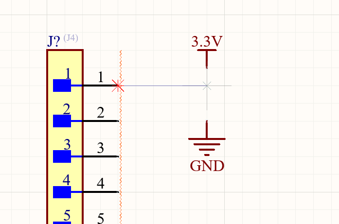
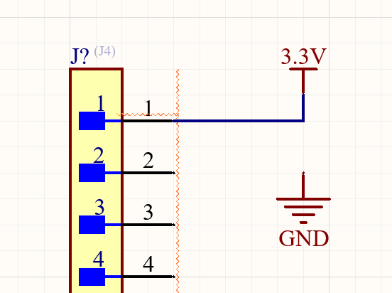
Note, for any components or wires on the sheet, you can remove them by selecting those objects and pressing delete on your keyboard.
In addition to wiring, you can place Net Labels on your schematic to connect two ports. Net labels are basically just wires, but without the physical traces going across the sheet.
To select a Net Label, navigate to the top tool-bar and select the wire icon. In the drop-down box, select Net Label.
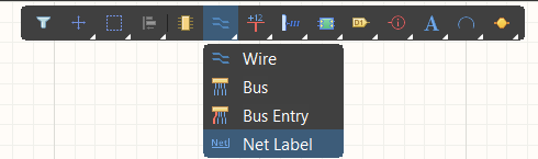
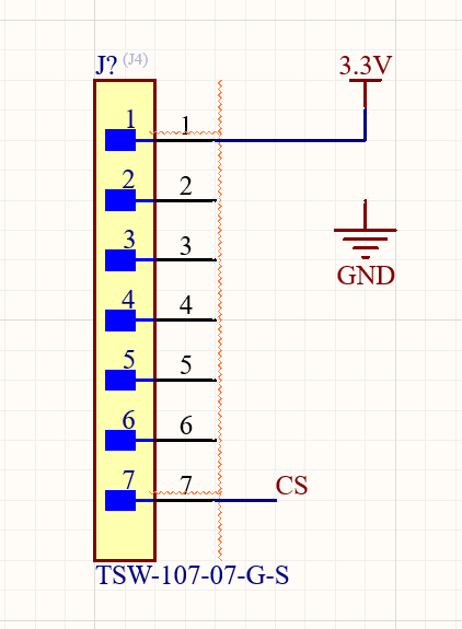
Attach the Net Label to port 7 on the 2x1 Header. You can left-click and drag the net label away from the port. When you do this, a wire will show, indicating the net label and port are connected.
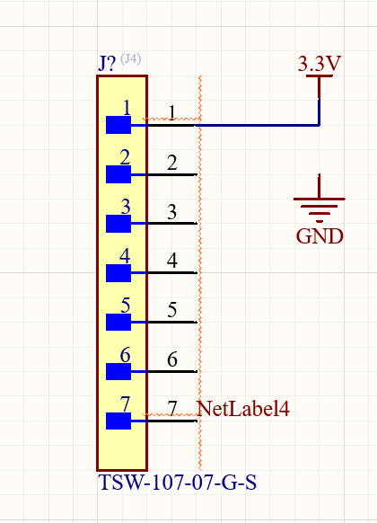
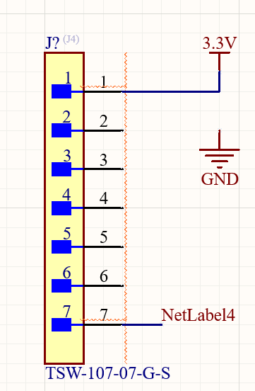
Now, double left-click on the newly placed Net Label, and rename it to "CS".
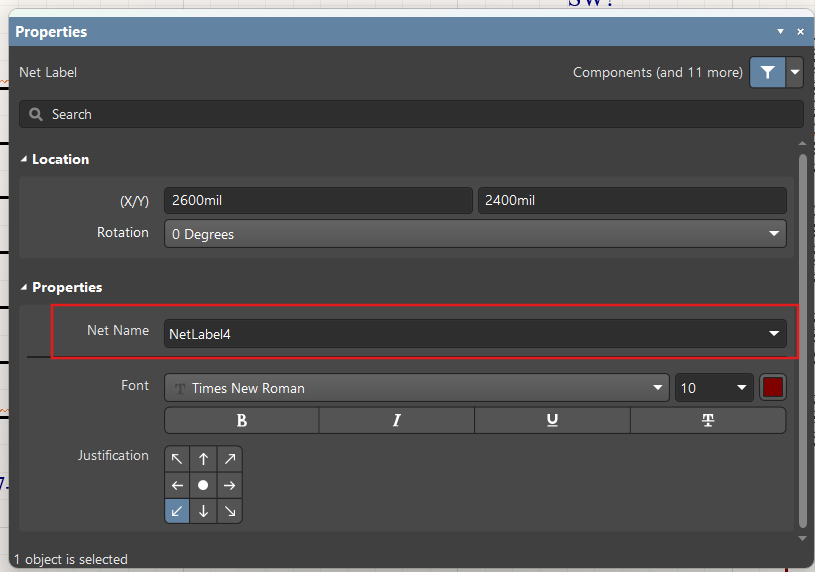
You should now have something similar to below:
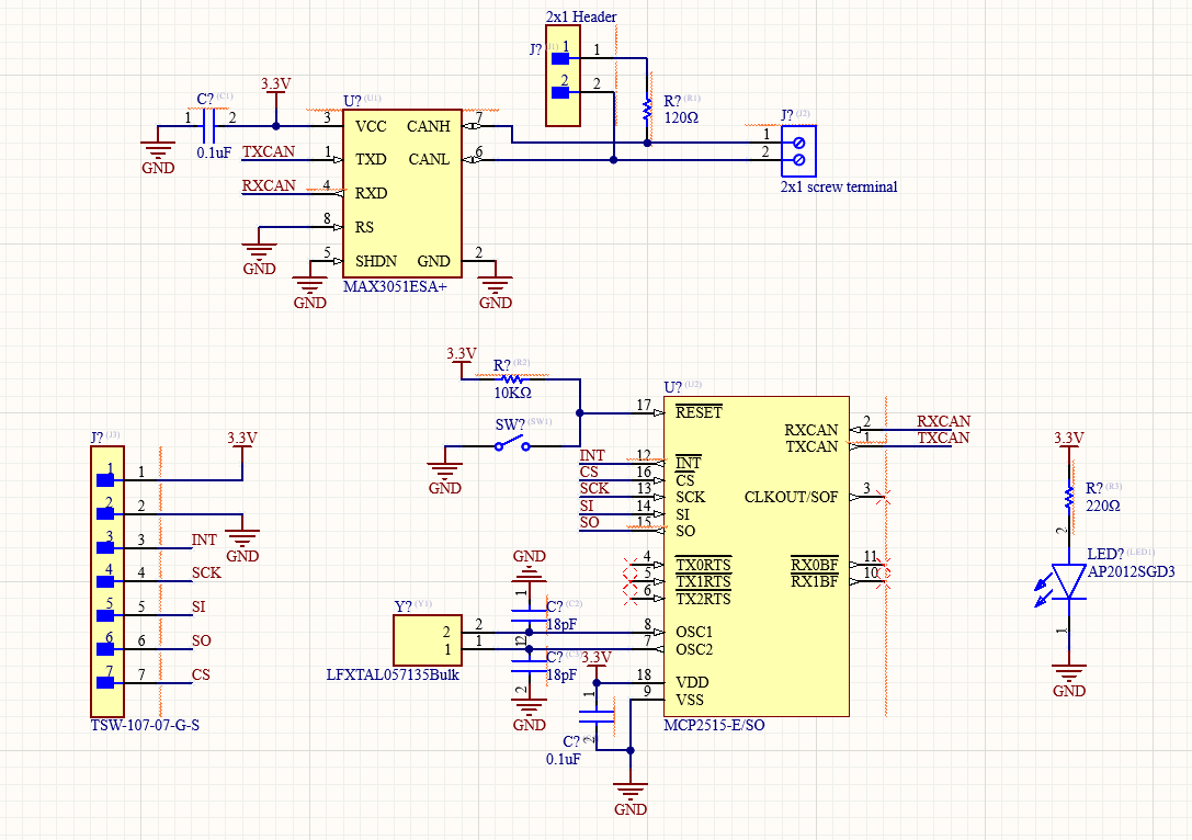
Using the tools you just learned, connect the components with wires and Net labels as seen below:
Note: when you complete your wiring, double-check your design to make sure everything is wired up correctly.
Schematic Annotation:
Once everything is wired up correctly, you're now ready to annotate your schematic. To do this, navigate to the top left tool-bar and select Tools --> select Annotation --> then select Annotate Schematics.
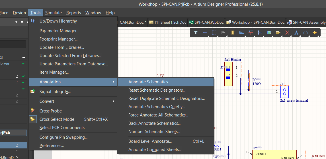
A new window should appear. You can modify how the annotation is laid out on the schematic.
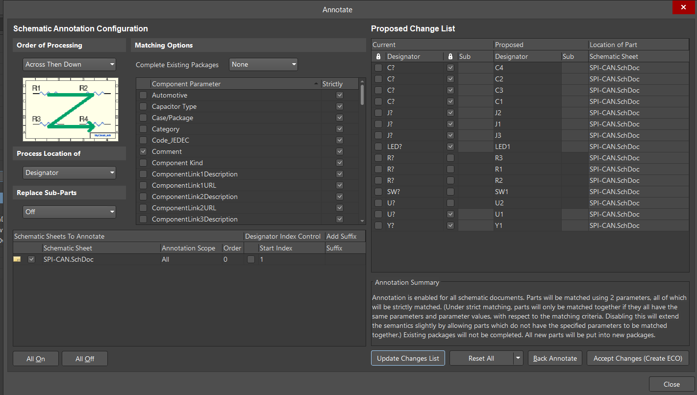
Once you're satisfied with the settings, select Update Changes List --> select OK --> then select Accept Changes (Create ECO). A new window should appear:
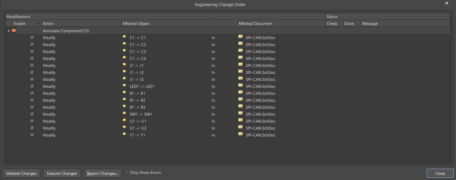
To finalize the modifications, select Validate Changes --> then select Execute Changes. Once the green checkmarks appear under each part's status, close out of both windows. Your schematic should now look like what's seen below:
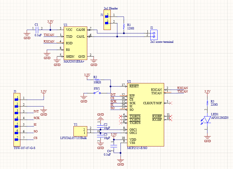
Now that your schematic is finished, you're ready to validate the design. Navigate to the Projects panel on the left side, right-click on the Workshop - SPI-CAN.Prj.Pcb icon, then select Validate PCB Project Workshop - SPI-CAN.Prj.Pcb.
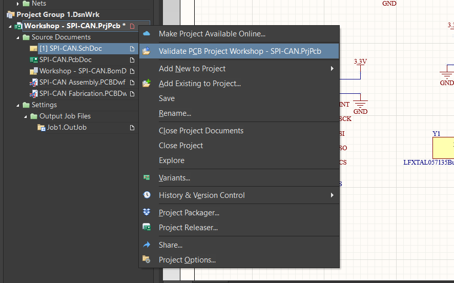
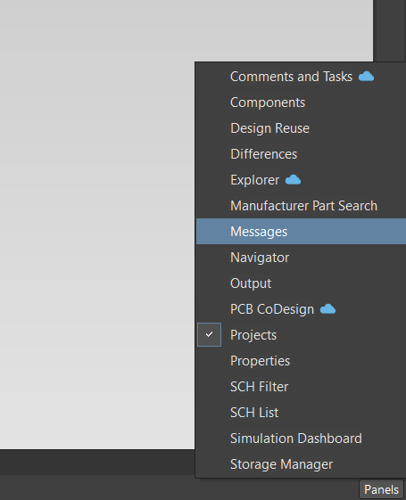
To chech the results of the validation, navigate to the Panels toggle and select Messages.
A new window should appear on the right side of your screen.
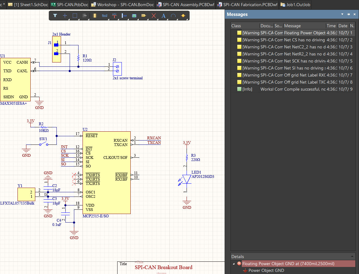
From the Electric Rule Check (ERC) validation, we received a bunch of warnings and an info block that tells us our design works. This is good! If you end up with messages that are proceeded with an orange box labeled Error, then you have some critical issues with your design that need to be fixed.
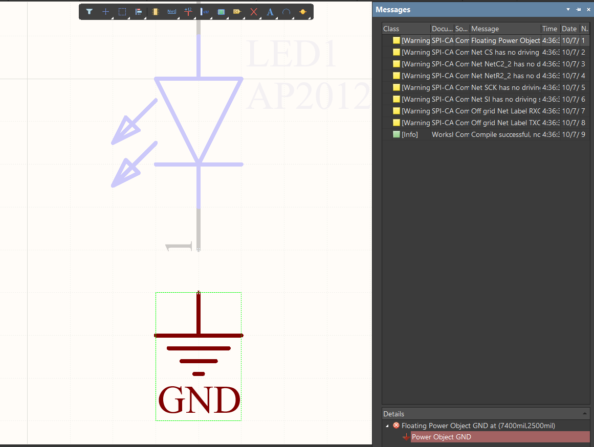
To tell exactly where an warning / error lives on your schematic, simply double left-click on the message. For instance, by investigating the message Floating Power Object, we see that there's a missing connection between LED1 and it's GND reference.
- We left this disconnected on purpose to see this appear in the validation check. Go ahead and insert the connection, then run the validation check again.
Upon opening Messages again, you'll see that the warning has dissapeared.
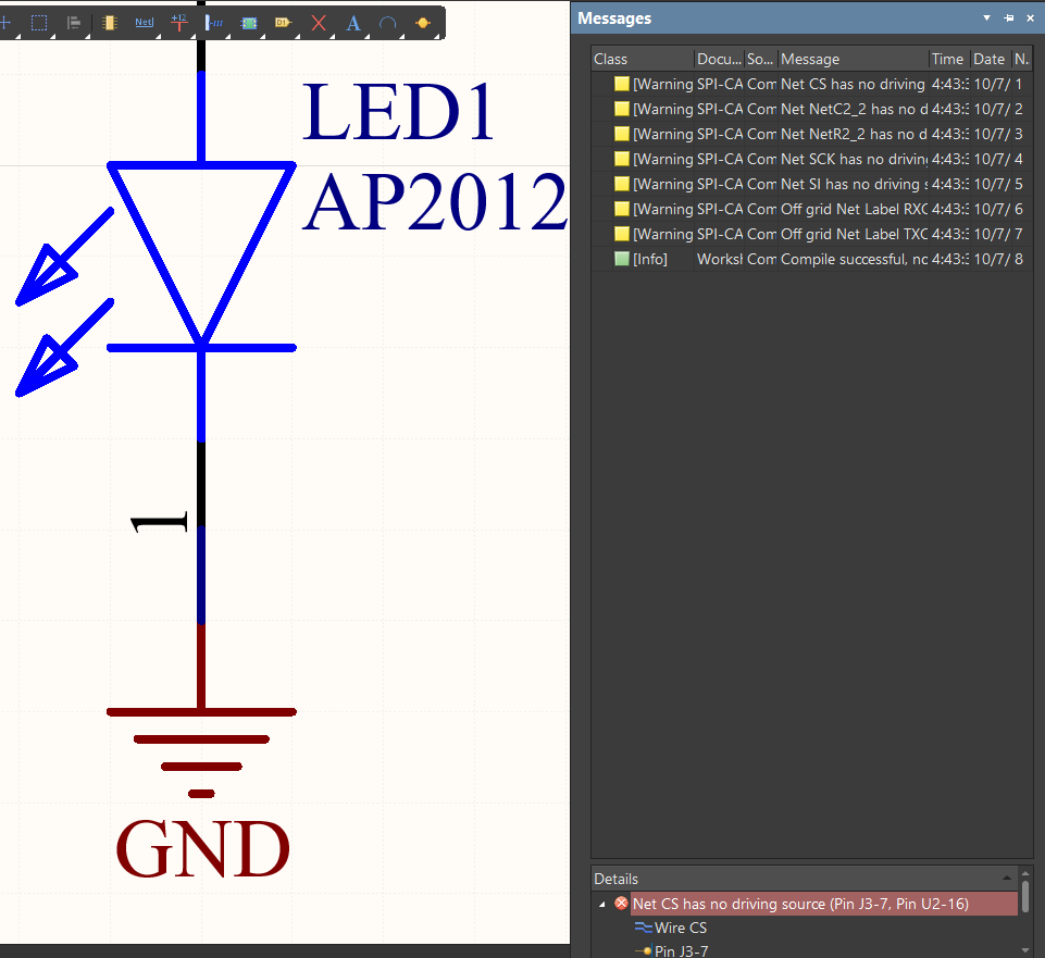
Now, we don't have to worry about the rest of these warnings for this design. Ideally, your designs should have no warnings or errors after validation.
Congratulations! You just created your first PCB schematic! At this stage, you'd typically allow our lovely SCR mentors and alumni to review your design and provide feedback for revisions. Fortunately, this design has alreayd been reviewed.
To learn about how to conduct a PCB layout, head to the next part of this tutorial: 3. Board Layout Pt. I