3. Board Layout
Introduction
After you complete a schematic, the next step in the PCB design process is to conduct the layout for your board. In doing so, you're translating the theoretical arrangement of your circuit design onto a physical board that will have to operate in the real world.
During the layout process, you'll follow the steps below:
- Board & Stackup: Outlining layers and arranging the via stack-up.
- Design Rules: Configuring the constraints of the layout to your the design requirements.
- Component Placement: Arranging components on the board and maximizing functionality.
- Routing: Connecting components together, sometimes between multiple layers.
- Design Rule Check (DRC): Verifying your layout confines to the requirements outlined previously.
Remember, there are many solutions for a design's board layout. It's your job to determine the best viable solution!
Layout Set-Up
Before you begin, keep in mind this tutorial is a continuation of the previous module's schematic.
- If you haven't already, please create the appropriate schematic by referring to 2. Creating a Schematic
To start, open the PCB document for the SPI-CAN Breakout Board project you created earlier. You should have a window similar to below:
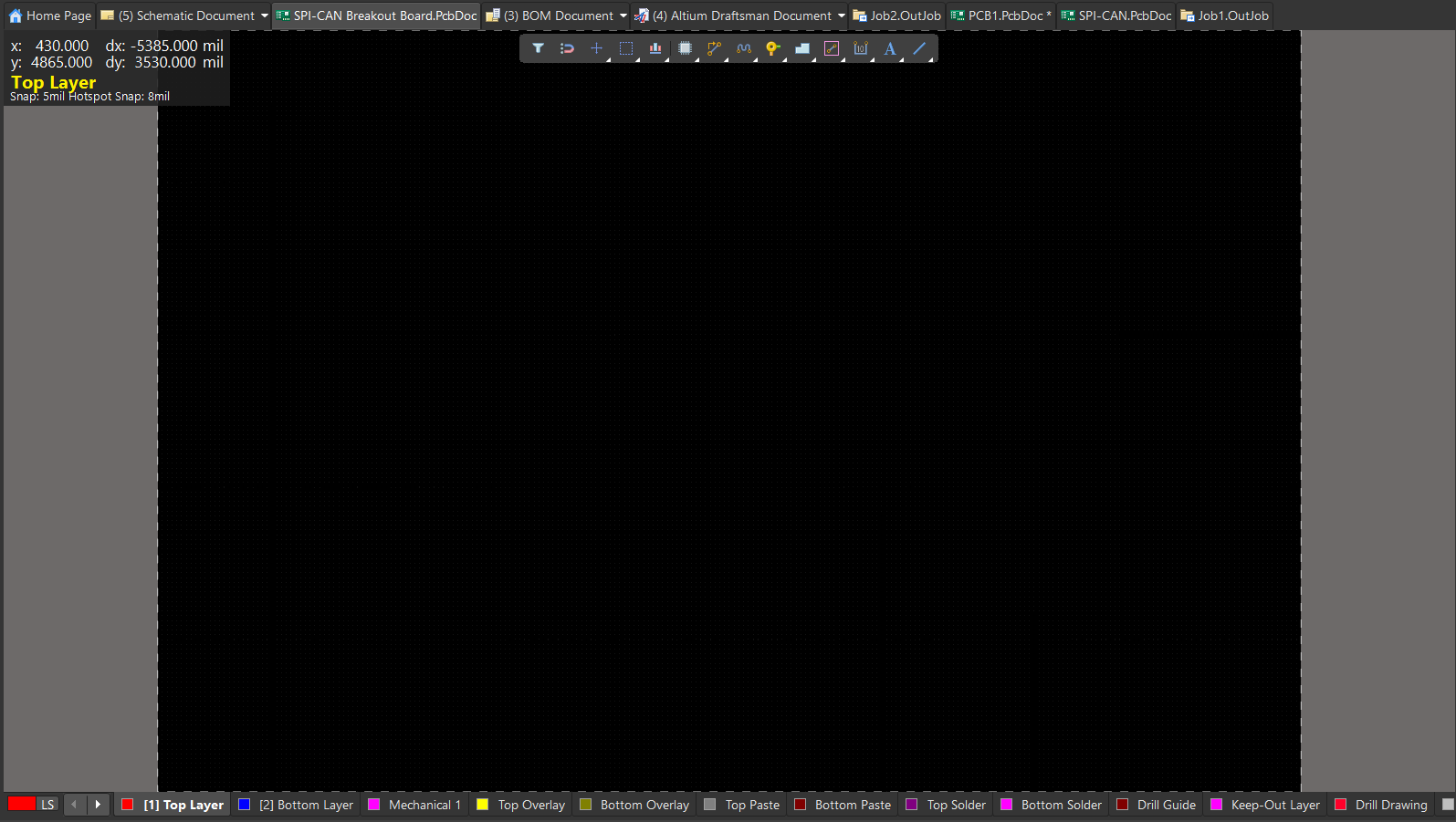
If you zoom out of the page slightly, you'll notice an odd cross-hair on the bottom left of the window. This is the origin, the reference point for your schematic's size. When placing down components at specific measurements, it's nice to have the origin level with your board.
To place the origin in the correct spot, navigate to the top-left tool bar. Then, select Edit --> select Origin --> then select Set.
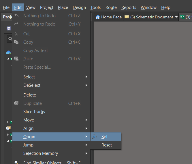
Now, a green cross should appear with your cursor. Place the green cross on the bottom right corner of your board border. Once your cursor is at the desired spot, use left-click to set the origin.
Note: You can use Ctrl + Mouse Scroll Wheel to zoom in on the corner!

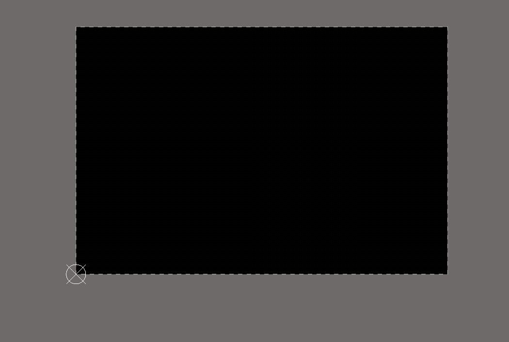
After zooming out, your layout should now look like what's seen below:
Now, since we only have about 15 components, we want to make out board smaller to save space and reduce manufacturing costs. To do this, we need to redefine the board shape.
In the top left tool-bar select View --> then select Board Planning Mode
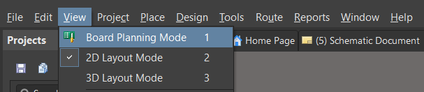
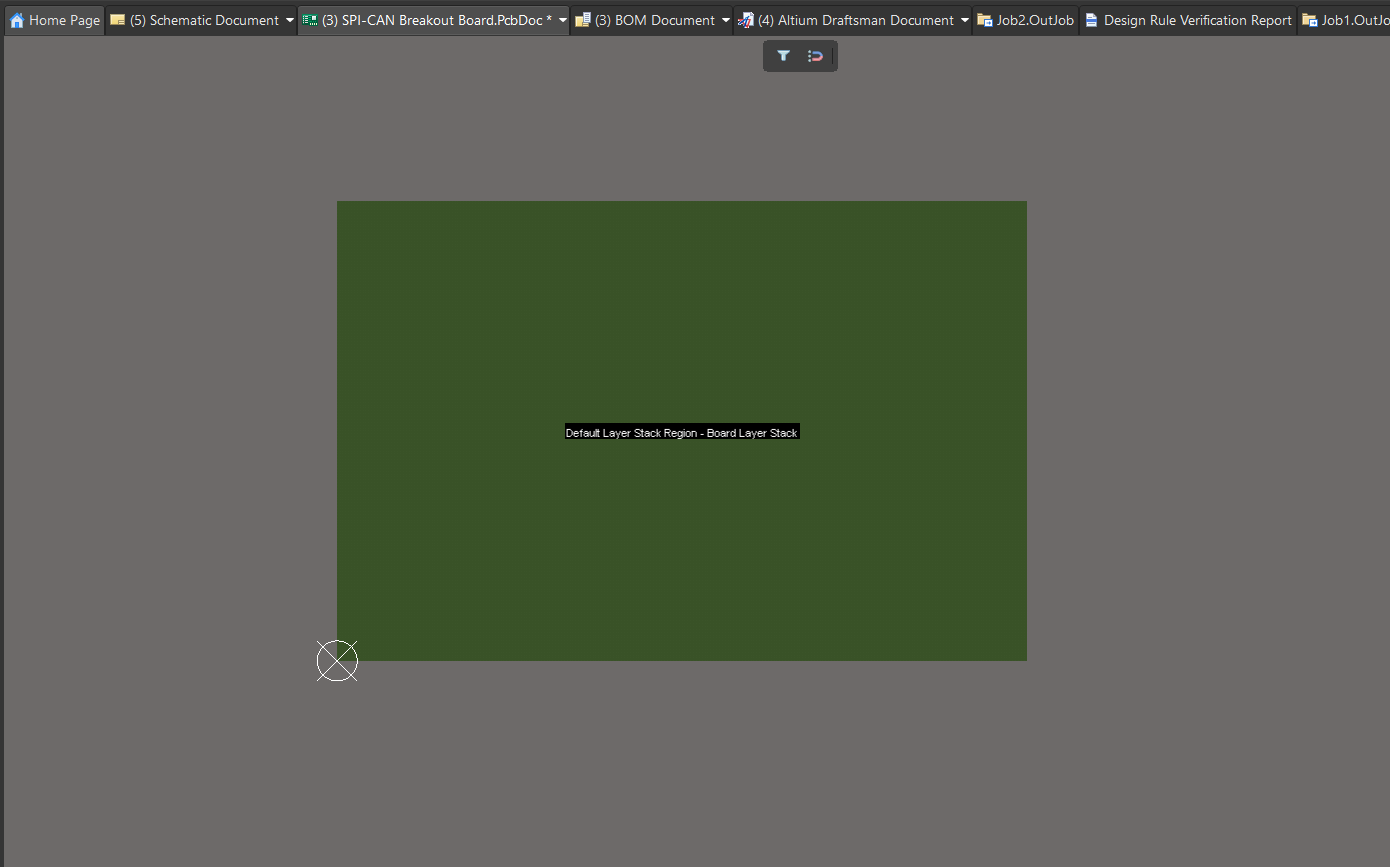
Your layout should now be in Board Planning mode, so your screen should look like this:
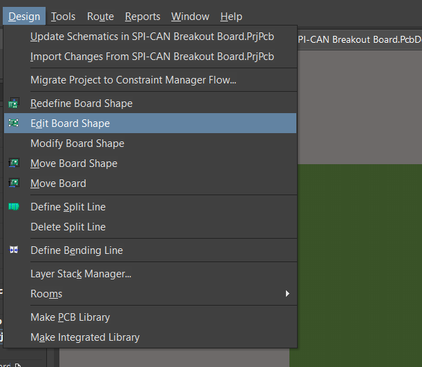
In the top left tool-bar, navigate to Design --> then select Edit Board Shape.
A white outline should appear around your board shape.
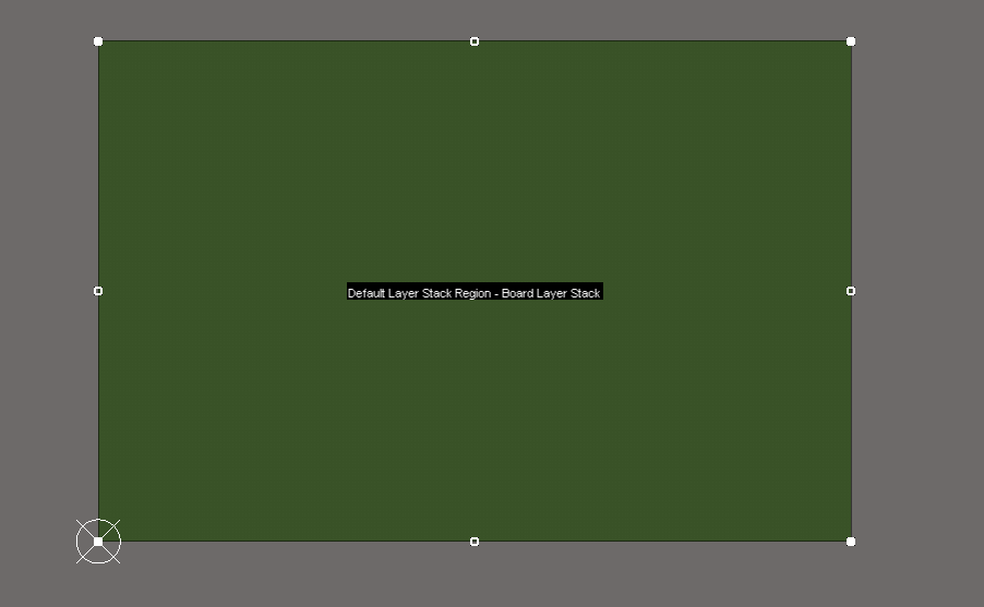
You'll want to change the board shape such that you have the following parameters:
- Length = 2000 mils
- Width = 1500 mils
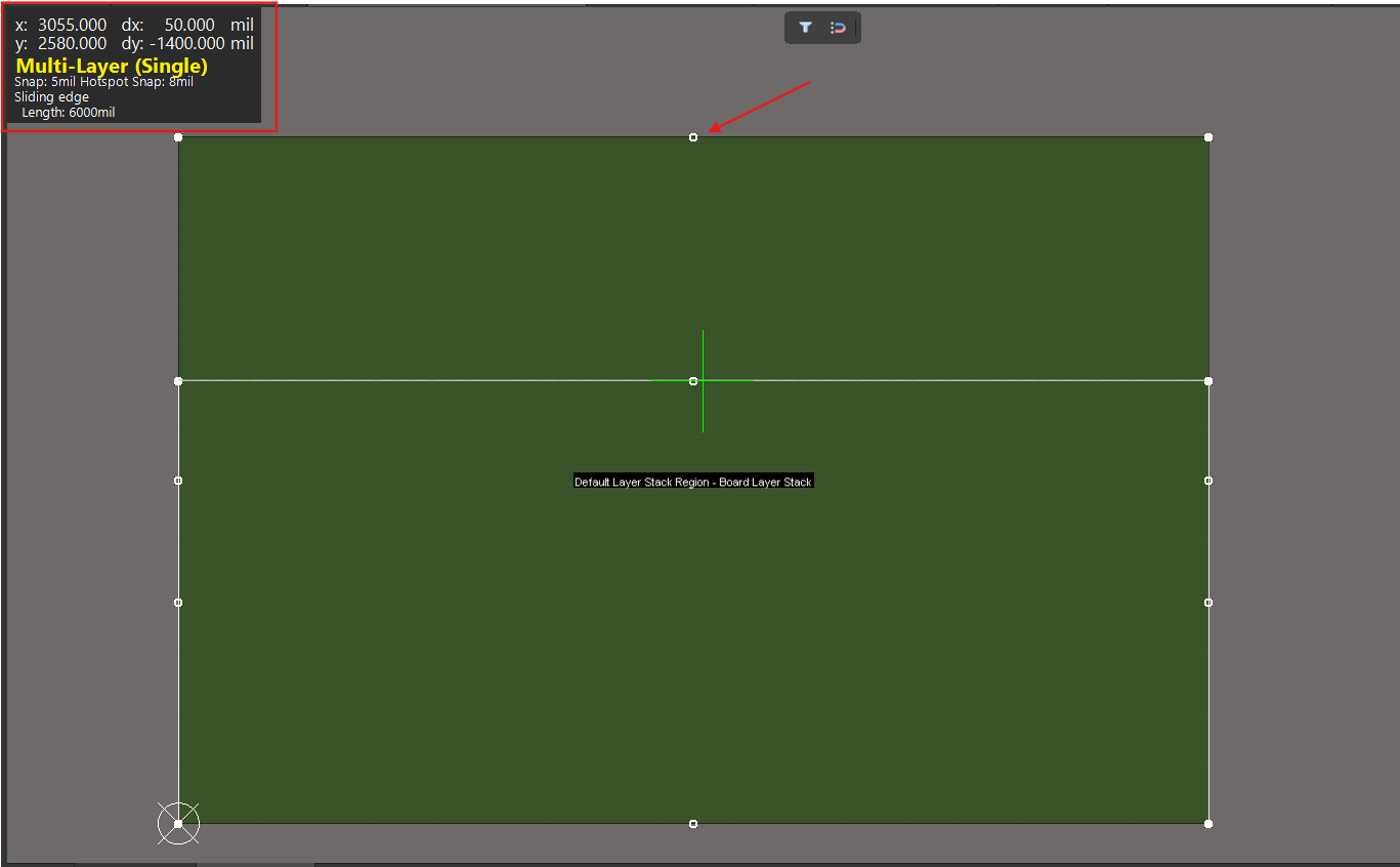
To change the board lengths, pick a side (top or right sides, move toward the origin) and select the center of the edge. Then, click and drag the edge until it's the correct size.
- Use the legend on the top left to determine when your side the correct size. Remember, you can zoom in to get a more precise placement.
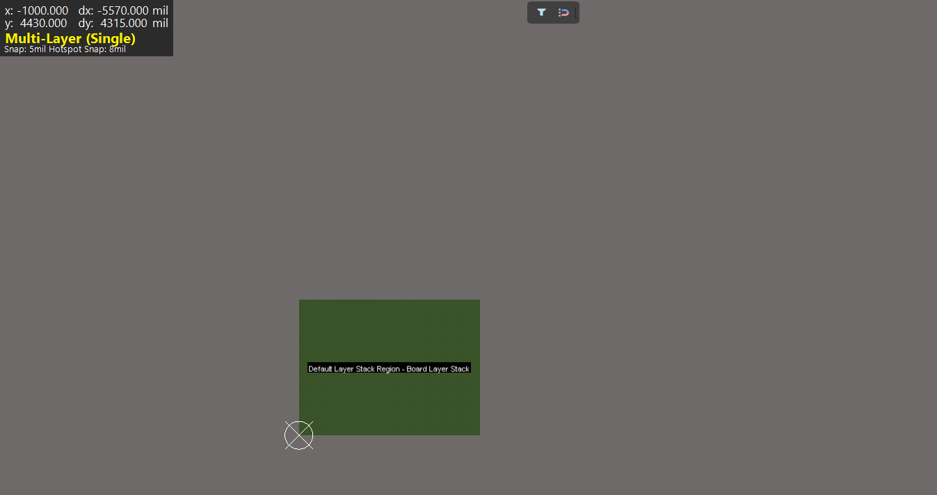
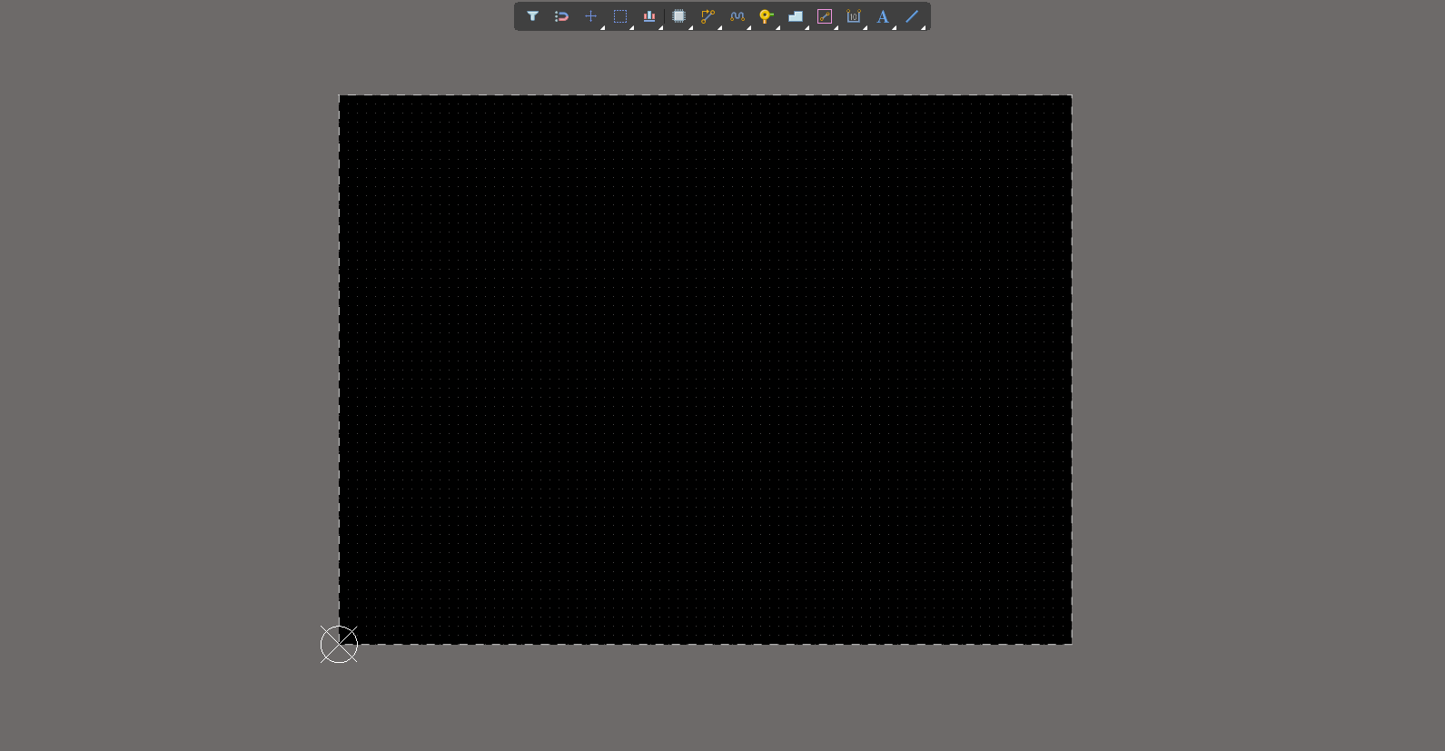
Once you're done, your board should be a much smaller shape.
Layer Stack-Up
With your board size ready, we can check our layer stack-up manager. For PCB design, it's important to consider how many layers or "planes" you want on your board.
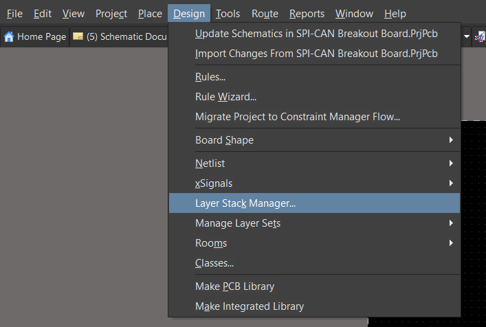
To view this, go to Design --> then select Layer Stack Manager.