
4. Board Layout Pt. II
Before you begin, this tutorial assumes you completed part I of the layout tutorial. You can find the tutorial by accessing this page: 3. Board Layout Pt. I
Component Placement
Before you can place your components, you must import your parts from the schematic you created. To import your components, navigate to the top left tool-bar, select Design --> then select Import Changes From SPI-CAN Breakout Board.PrjPCb.
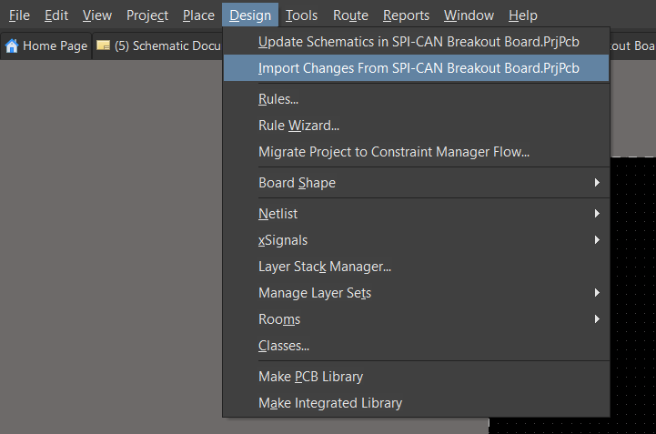
A new window will appear showcasing which componens and nets will be added to the layout.
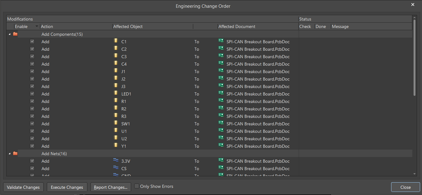
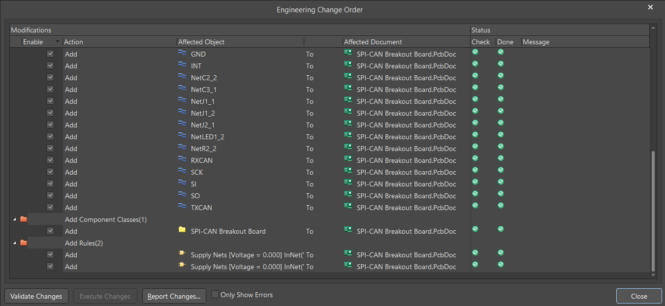
Go ahead and select Validate Changes, then select Execute Changes. Green checkmarks will appear under the Check and Done columns, indicating if a component has been successfully imported.
Upon closing the window, your parts will appear on the layout as shown below:
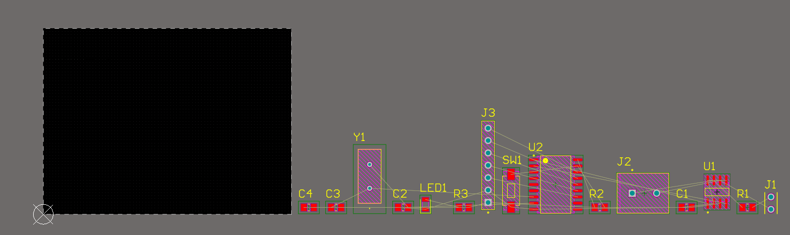
Typically, you can click and drag components into your board dimensions. For the sake of time, we'll use a different technique for placing components by having our schematic and PCB documents open side-by-side.
Start by having only two windows open: your schematic and your PCB documents.

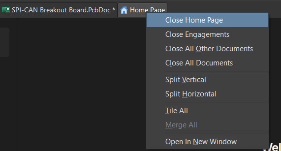
To close a window, right-click on the window you want to close, then select Close [Window Name]
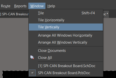
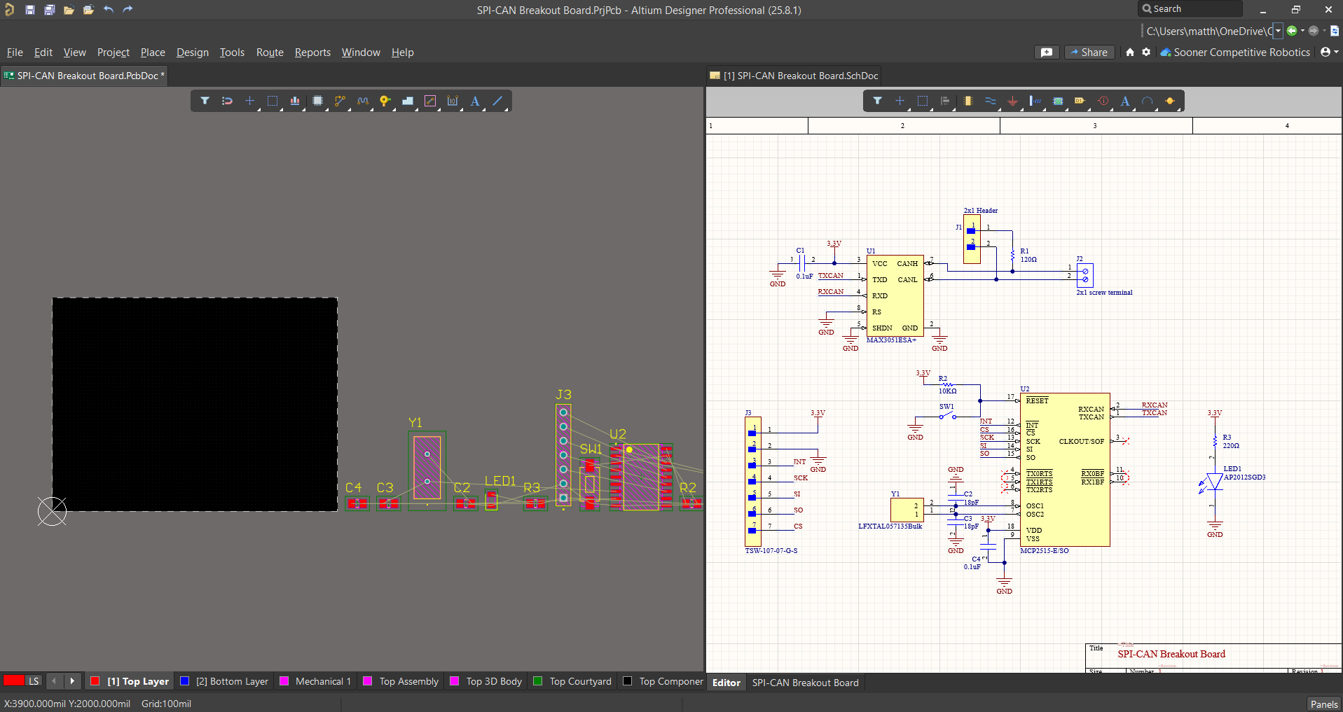
Now, your Layout and Schematic should appear side-by-side one another.
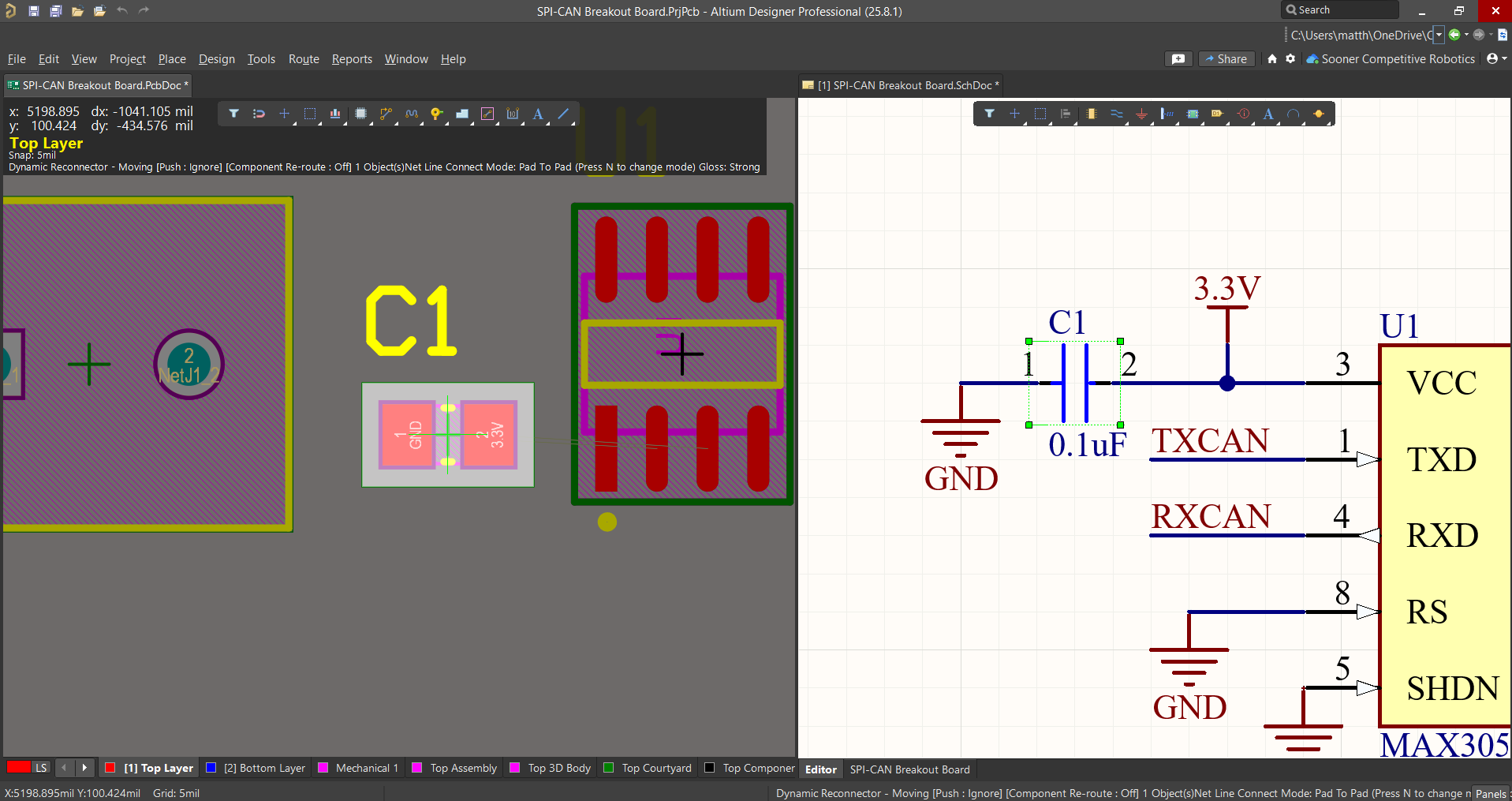
This way, by selecting a part on the schematic, Altium will automatically select the same part on the PCB layout.
Using this technique, arrange the components on the layout as seen below. Remember, there's multiple ways to conduct this layout, this is just one of the solutions.
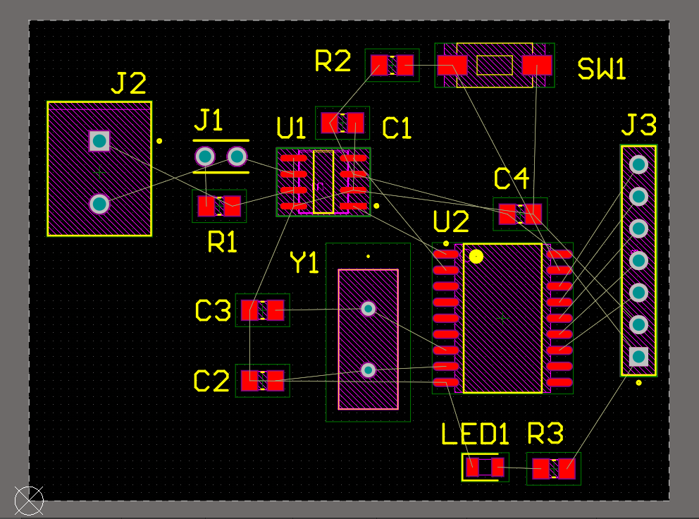
Note: in layout design, it's important to keep "friendly" components close together for high functionality. I.e., keep your decoupling capacitors close to the device they're decoupling, etc.
Layout Routing
Once you have your components arranged, you'll start wiring your components together through tracing.
Tracing is connecting solder masks together on a PCB using thin copper lines. These lines carry current between your components. Think of them as flat wires on your board.
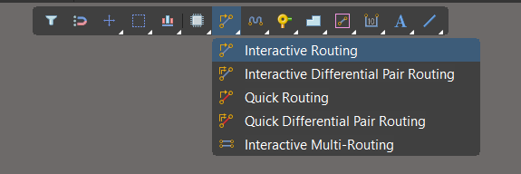
To trace your components together, you have a couple of options. First, you can navigate to the toolbar with the various icons, right-click on the middle icon (the diagonal line with the arrow), then select Interactive Routing.
- Another way to access the trace feature is by holding Ctrl + W on your keyboard.
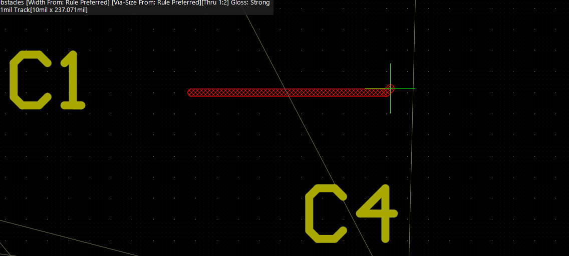
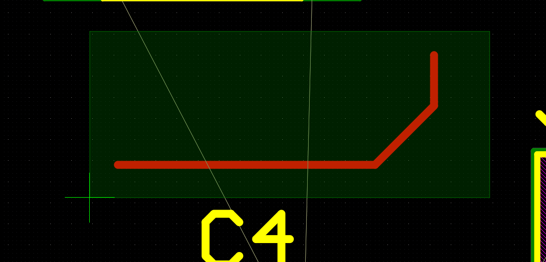
A green cross will now appear with your cursor. When you left-click on your layout, a red line will appear from the spot your selected. This creates a faded trace waiting to be place.
Upon left-clicking again, that part of the trace will be placed on the layout. From the second spot you selected, another part of the trace will begin appearing. To finish placing the trace, press esc on your keyboard.
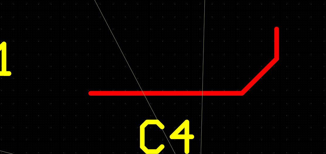
Since this trace is floating, we don't need it for our design. To delete a trace, select the entire trace by holding down left-click and highlighting the entire object. Then, select delete on your keyboard.
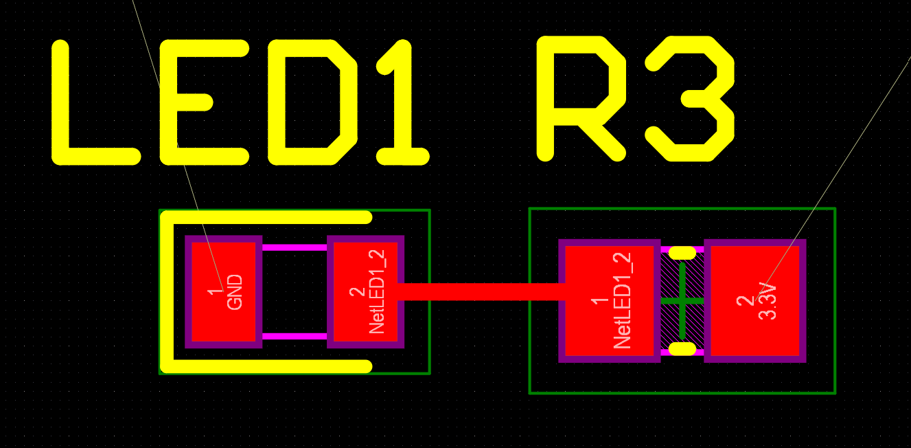
Let's practice connecting a trace between two pins. Navigate to the bottom of the layout and find LED1 and R3.
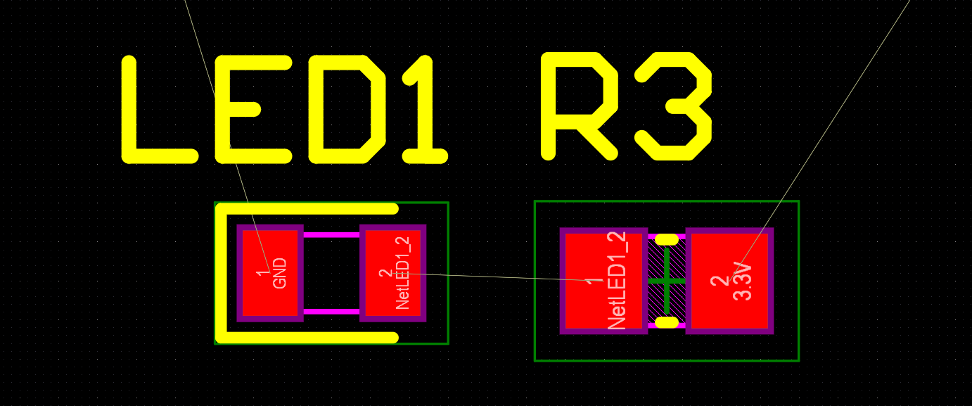
We'll route these two components together. Notice how there are thin gray lines connecting between pins of specific components. These thin lines tell you which pins need to be routed together. If you Zoom in on a component, you can read the Net associated with it's pins.
Between LED3 and R3, we see they both have the LED1_2 net.
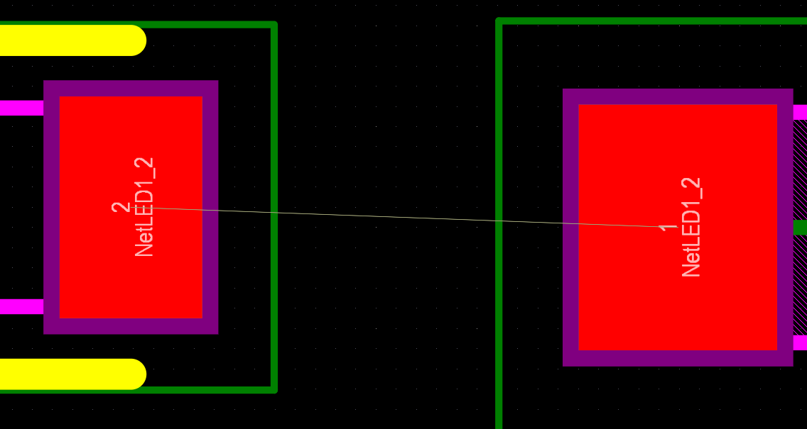
To trace these pins together, activate the routing tool. Then place the start of your trace on either pad. You'll notice when you hover over the center of a pin, your cursor will snap onto the center with a green cross hair.
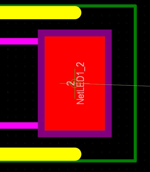
Now, drag your trace across the layout onto the second pin from R3. You should get a faded trace like below:
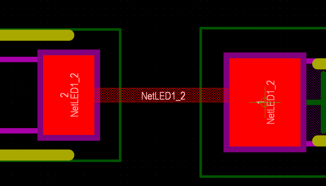
Left-click on the second pin whenever the cursor snaps over the center of the pad. Now, you should have a completed trace.
One thing to keep in mind when routing is to ensure your signals travel across the path of least resistance. This means setting up your traces at bends with 45 degree angles. A trace that bends at 90 degrees creates signal inflections in your design, causing increased electro-magnetic inteference (EMI) and impedance discontinuties.
The picture on the right is a much better example of routing compared to the left.
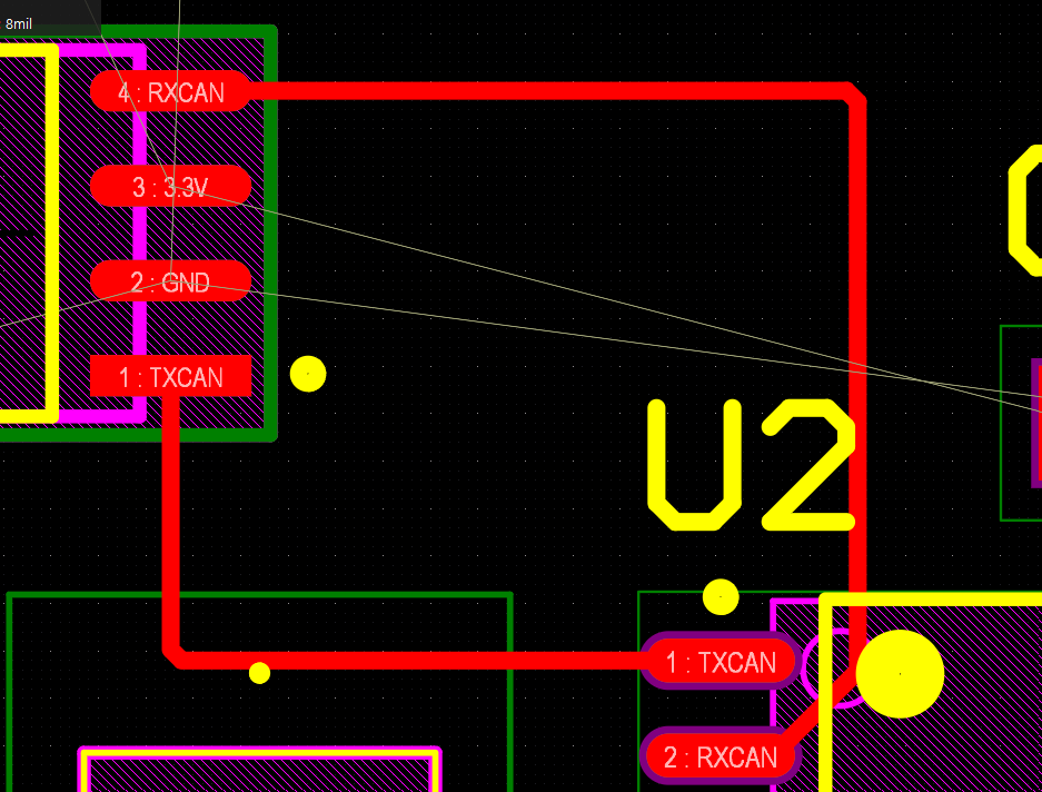
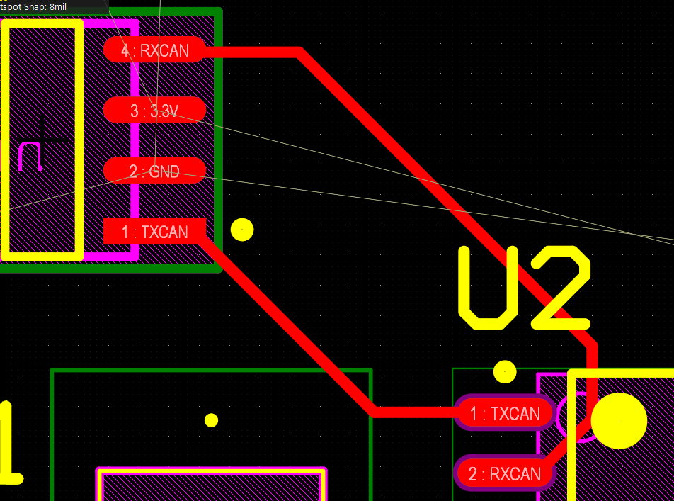
Note: in actual layout design, it's important to use differential pairing on signals that operate at the same frequency (For instance, signals TXCAN and RXCAN from U2). This can help mitigate issues with cross-talk and EMI. For our purposes, we won't consider this issue. But, keep this in mind!
Now, use the techniques you just learned to conduct the routing between all of your signals nets as seen below:
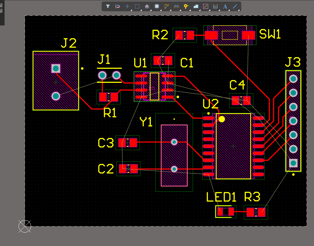
You can also route between signals on different layers of your board. For instance, let's route two signals on the bottom layer.
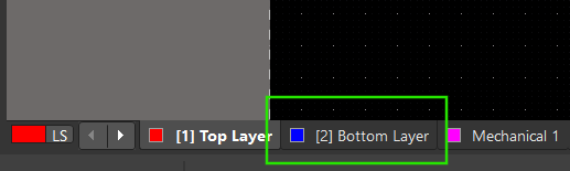
Next, route the NetJ1_2 signal between your J1 and J2 components. You'll see the trace appear in blue as seen below.
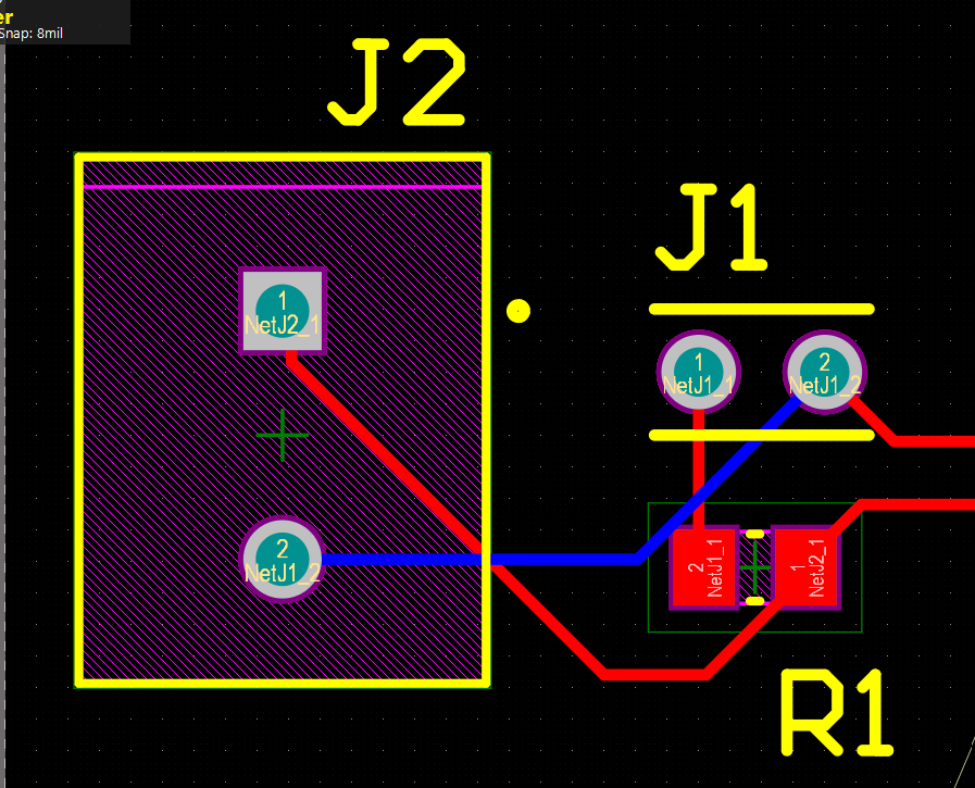
Notice how the blue trace went under the red trace. This is extremely helpful if a pin you're routing is blocked by existing traces on the same layer.
Note: this only works easily for through-hole pins. connecting a trace from another layer on a surface-mount component (like R1) won't work! To go around this, you have to place a Routing Via next to your surface-mount component before tracing on a different layer.