
PCB Design Guide
PCB Design Guide
Introduction
This guide is not a “How to Use Altium” document. Instead, it focuses on layout design practices and considerations that go beyond what’s covered in the standard onboarding process. It assumes you’re already familiar with basic Altium navigation and PCB creation. If you’re new to PCB design or still learning how to use Altium, refer to the onboarding documentation.
The two-layer board design section is written with beginners in mind. It simplifies explanations and avoids deep technical reasoning to minimize confusion. In contrast, the four-layer board design section was written for those who have already completed at least one two-layer board in SCR. It provides more detailed insight into design choices and introduces advanced layout considerations / techniques. To avoid redundancy, many of the foundational concepts from the two-layer section are not repeated in the four-layer section. If you're designing a two-layer board that involves more advanced routing or layout strategies, the four-layer section may help in certain cases.
Before modifying any documents, change the project file name, schematic file names, and PCB file name to reflect the project you are working on. Generally, it should follow this format:
At the very least, capitalize the first letter.
Schematic Formatting
Before placing any components or starting a design, modify the labels on each schematic document to reflect the project you are working on:
Master Sheet, Sheet Symbols and Ports
The master sheet is how you connect signals across different sheets. Every time a new sheet is added, you must generate the sheet symbol.
To connect signals across sheets, you use ports.ports. These function the same as net labels, but must be added to your sheet symbol in the master document. If you end up having a signal that is in two separate locations on one sheet, but needs to connect to another sheet, use a Port to connect to the other sheet and use a Net Label to connect it within the same sheet.
When using net labels or ports, utilize snakecase and all capital letters to label your nets. Also, make your label descriptive enough so that others besides you know what it is.
This ensures the label is easy to read and is consistent throughout the design.
Circuit and Component Labeling
Major circuitry and components should be labeled by either a technical name or product name. They should also be separated by space or lines from other circuits or components.
Parts that require values (capacitors, resistors, etc) should have their values labeled as well.

Labeled Resistors in Schematic
PCB Revision Notes
While we do have a version control system, it is suggested to use a notes box at the top corner of a schematic to document major changes.
Differential Pairs
Differential pairs are two traces that carry equal and opposite signals—used for high-speed or noise-sensitive communication like USB or Ethernet.

Differential Pairs in Schematic
In Altium Designer, you define differential pairs by assigning nets a common prefix (like USB_D+ and USB_D-) and placing the differential pair designator on the net.
Schematic Design Standards
Decoupling Capacitors
Every IC / microcontroller / voltage output should have at least one decoupling capacitor next to its power pin. The purpose of these is to filter out high frequency noise and ensure local voltage stability.
These are smaller (usually 0.1 uF), but check the datasheet to see if the manufacturer requires more than that value or more capacitors. These are usually 0805 capacitors, which are the generic capacitors in the Sooner Competitive Robotics part library.
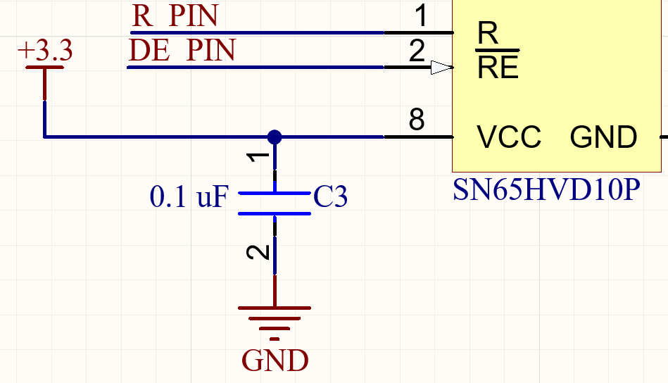
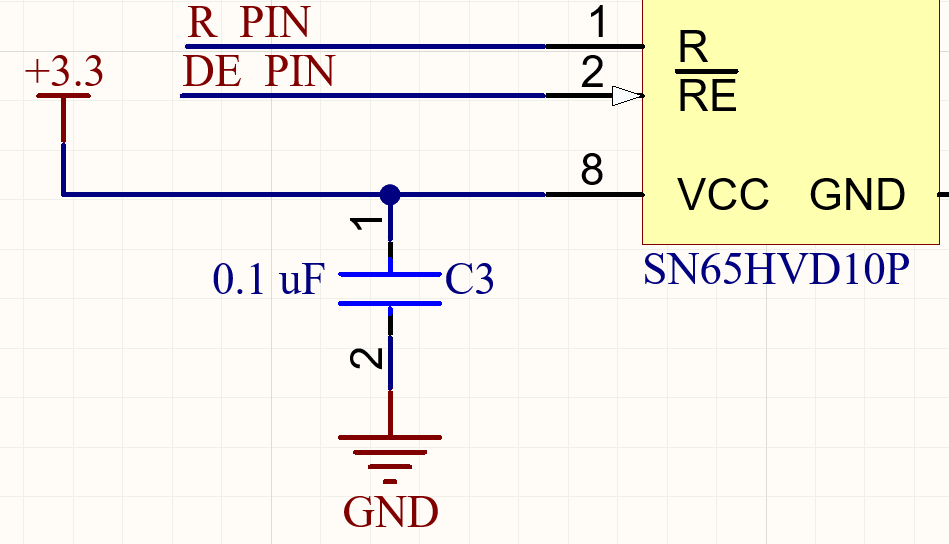
Decoupling Capacitors in Schematic
Bulk Capacitors
Bulk capacitors are similar to decoupling capacitors in that they should be placed close to the IC, microcontroller, or voltage regulator output—but they serve a different purpose. During sudden load changes, if there isn’t a nearby charge reservoir, the power supply may not respond quickly enough to maintain voltage, especially if the power trace is long or inductive. This can lead to a brownout, where the voltage drops drastically and may cause the microcontroller or other digital logic to reset, crash, or behave unpredictably. These capacitors are usually large (10 µF10 μF to 1000 µF)1000 μF), depending on how much current the system demands and how quickly that current may change. The 10 uF capacitors can come in the 0805 package, but larger values may require larger package sizes.
Power Input Protection
Whether it is for a linear dropout regulator (LDO) or for a buck converter, a Schottky diode and transient voltage suppression diode (TVS) should be on the input.
The Schottky diode should be in series and the TVS diode should be in parallel. The TVS diode should come before the Schottky diode. Beginners should ask an experienced member about how to select these. Odds are, depending on the situation, that there are parts that are used across every board.

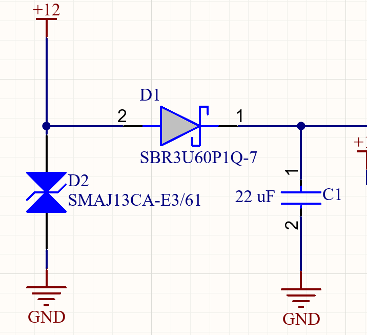
TVS Diode and Schottky Diode in Schematic
Test Points
Add a way to easily probe important or key signals.
Unfinished: Need walkthrough of how to do this.
Two Layer Board Design
Two Layer Overview and Definitions
The two-layer PCB allows designers to route on the top and bottom layer. These are cheap, inexpensive, and will probably be the most common board stack-up used in SCR.
Below are a few definitions that will be useful when reading through the sections (and you should be familiar with):
Board Shape and Size
This is largely dependent on design, but most boards should resemble a rectangle or square and stay within 100mm x 100mm (3937.01 mil x 3937.01 mil). If the board becomes any larger than this, it ends up being more expensive. So, attempt to keep it within this range. If your board ends up being larger than this, make sure that you are utilizing board space adequately.
Component Placement Considerations
When placing components on a PCB, start by positioning connectors like USB ports, power jacks, or headers where they need to be—usually along the edges or corners of the board. Next, group related components close together; for example, keep resistors near their associated LEDs or place capacitors right next to the microcontroller pins they support. Try to orient similar parts in the same direction to make the board neater and easier to work with.
Make sure not to cram components too tightly; leave enough space between them so you have room to route traces later. Decoupling capacitors, especially small ones like 0.1 µF,μF, should be placed as close as possible to the power pins of integrated circuits to reduce electrical noise.
Don’t forget to leave space for mounting holes if your board will be screwed into a case or enclosure!
One way to organize your PCB is to think of each type of IC or circuit as a “city”. Place things that are alike close to other things that are alike and align them accordingly. For example, if you have two linear dropout regulators (LDO) that supply different voltage levels for your PCB, they should be relatively close in proximity to each other and have a similar layout in regards to their local capacitors.

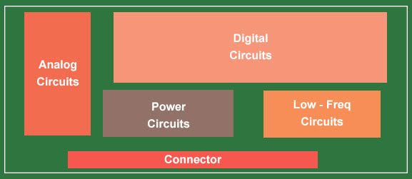
"City"-Style Component Placement
Two Layer Routing Priority
When you begin routing your PCB, it is important to route things in order of importance to ensure short and direct traces for critical signals.
Two Layer Trace Width
Trace width is how wide the copper lines (traces) are on your PCB. Just like pipes, wider traces can carry more current. If a trace is too thin for the amount of current flowing through it, it can heat up, cause voltage drops, or even burn out.
Here are some simple starting suggestions:
Vias
Similar to copper traces, vias—the small plated holes that connect different layers of a PCB—need to be sized based on how much current will flow through them. Vias allow electrical signals or power to travel between layers, such as from the top layer to the bottom layer of a two-layer board.
For communication and low-power signals like GPIO, I²C,I2C, or SPI, only a tiny amount of current is used, so small vias are perfectly fine. A typical signal via might have a hole size of 0.3 mm (12 mils) and a pad size of around 0.6 mm (24 mils). These save space and work well for most digital signals.
However, for power lines or high-current paths, you need larger vias to handle the increased current without overheating or causing voltage drops. For example, a via carrying up to 0.5 amps might use a 0.4 mm hole with a 0.8 mm pad, while anything above that (up to a couple amps) may require 0.5 mm holes or more—and possibly multiple vias in parallel.
Polygon Pours
Instead of drawing many thin traces for ground and power connections, you can just "pour" copper in unused areas and connect it to ground or power automatically. This helps keep the circuit more reliable and clean. Your bottom layer should have a ground pour that extends across the entirety of the PCB to ensure proper grounding. Once this is done, you can access the ground on the bottom layer by using a via and assigning it to the ground net. For power, depending on what voltages are present, you can place polygon pours to connect all of your peripherals accordingly. Polygon pours can be any kind of abstract shape, but try to make it as clean as possible and make sure that you are sufficiently connecting everything.

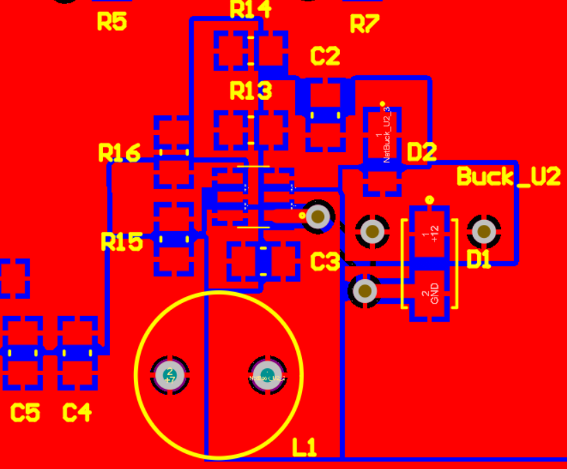
Polygon Pours Connecting a Buck Converter's Inputs and Outputs
By default, Altium’s connection type for polygon pours is called a “spoke” connection or thermal relief. Whenever you connect a polygon to a net, each side that is exposed to it should have a spoke. If not, then rearrange the surrounding parts or resize the polygon to ensure proper connection. If you are unable to do this, then switch to routing that net with a regular trace.

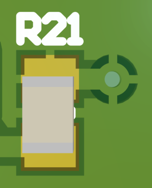
Thermal Relief / "Spoke" Connection
Mounting Holes
For mounting holes, place a pad and make the hole size larger than the copper size.

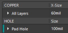
Mounting Hole Configuration
Bellow is a table showing some common metric screw sizes used by SCR and different "fits" for hole sizes. It is typically recommended to do the normal fit or loose fit for PCBs. M3 screws are the most commonly used screw for PCB mounting holes.
| Screw Size (M) | Nominal Dia (mm) | Close Fit (mm) | Normal Fit (mm) | Loose Fit (mm) |
|---|---|---|---|---|
| M1.6 | 1.6 | 1.7 | 1.8 | 2.0 |
| M2 | 2.0 | 2.2 | 2.4 | 2.6 |
| M2.5 | 2.5 | 2.7 | 2.9 | 3.1 |
| M3 | 3.0 | 3.2 | 3.4 | 3.6 |
| M4 | 4.0 | 4.3 | 4.5 | 4.8 |
| M5 | 5.0 | 5.3 | 5.5 | 5.8 |
Four Layer Board Design
Four Layer Overview and Definitions
Four layer PCBs offer many benefits over a two layer PCB, many of which will be discussed throughout this chapter. With a four layer board, the inner two layers can technically be whatever the designer chooses. But, for simplicity sake and to prevent issues, the four layer stack-up for SCR will be (top to bottom):
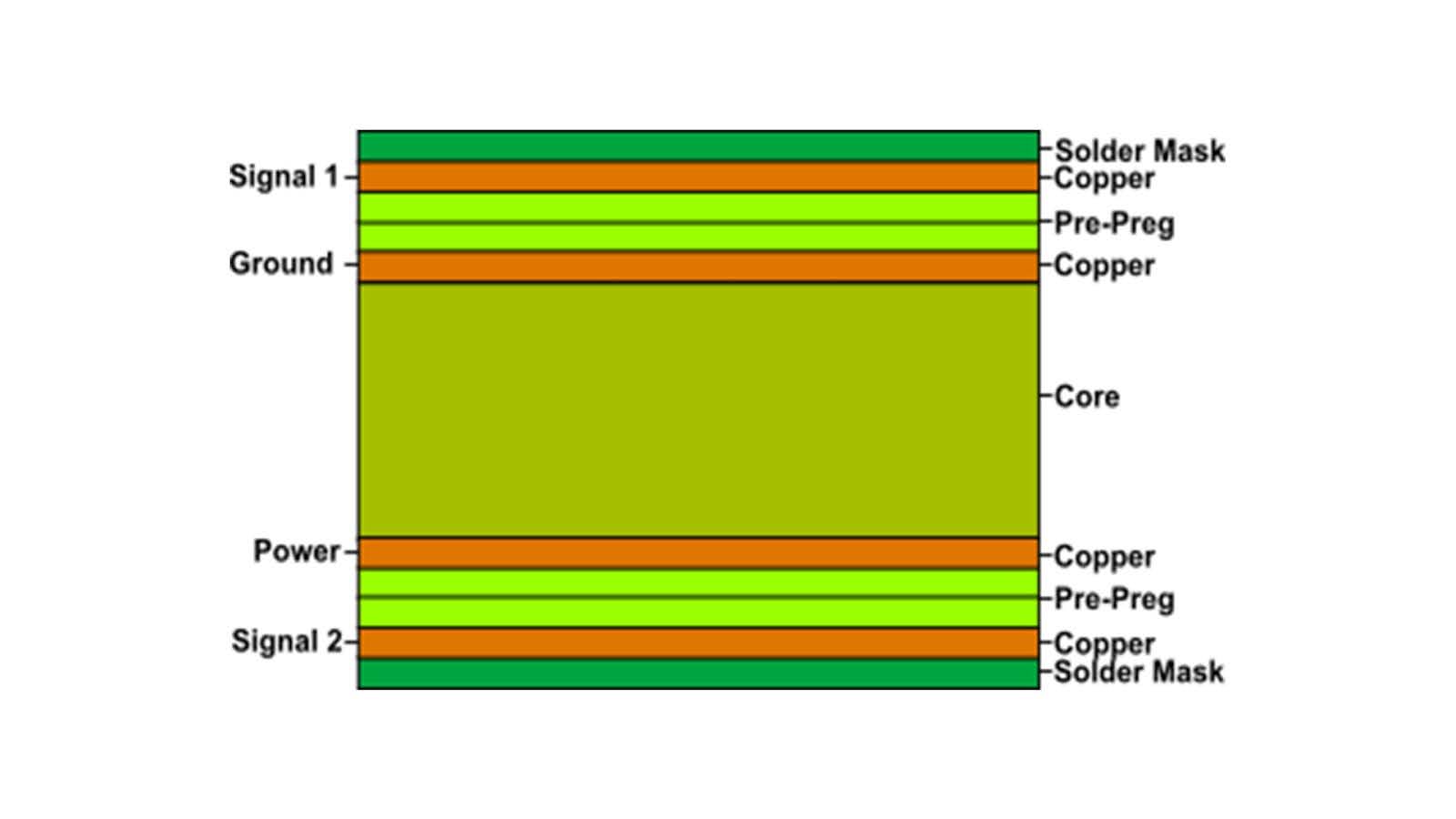
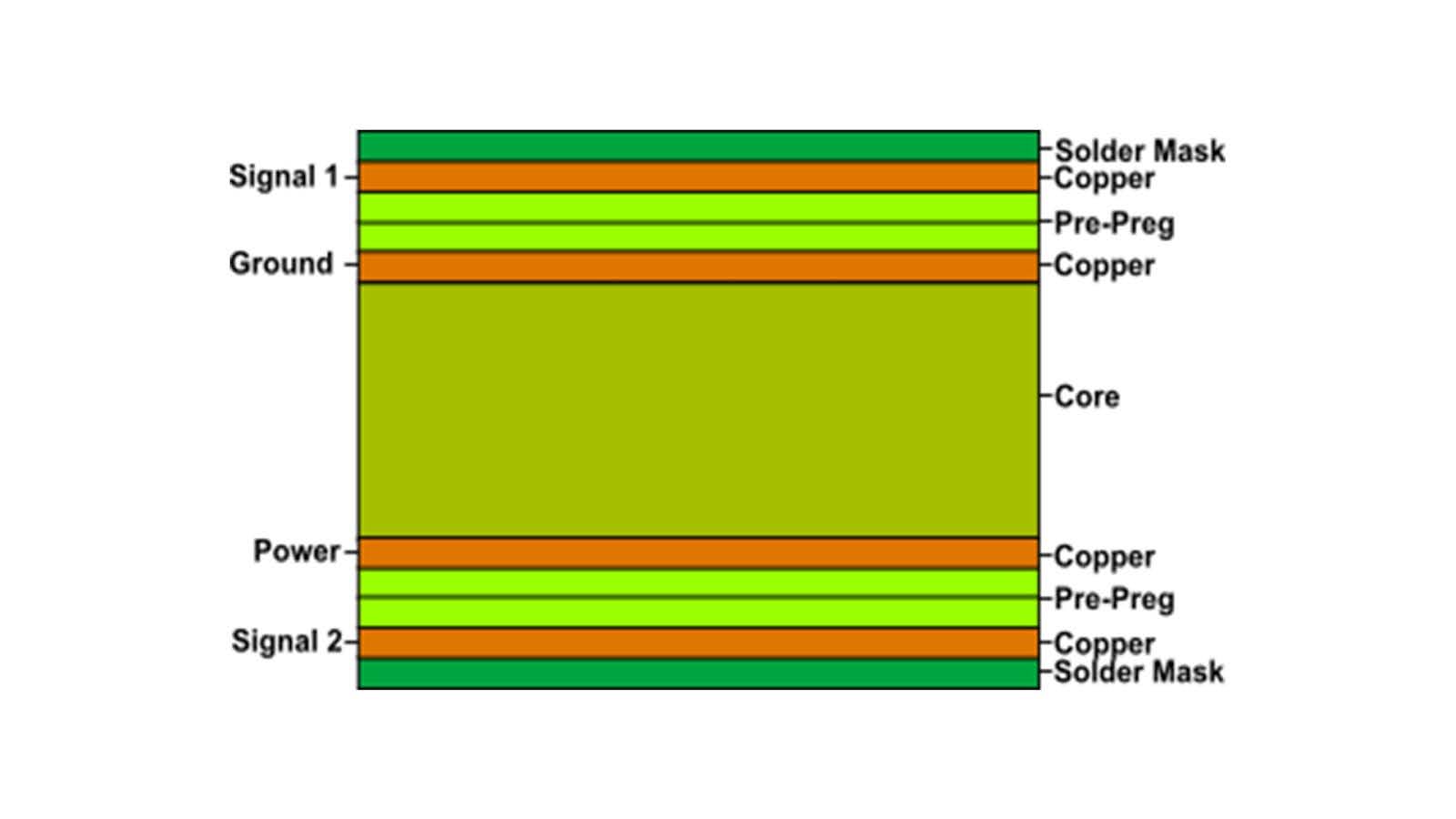
Four Layer Stack-Up Visualization
Before discussing all of the considerations for routing a four layer board, some important definitions are needed for understanding why certain steps are taken:
Important Four Layer Rules
Four-layer PCBs offer significant advantages: they streamline routing, make it easier to manage signal integrity, provide clean return paths that minimize current loops, and make impedance matching far easier than on two-layer boards.
To preserve these benefits, traces should NEVER be routed on the dedicated ground or power plane layers.
While a single small trace on a power plane might not cause catastrophic issues, routing multiple or critical signals on these layers introduces serious problems:
Four layer boards are slightly more expensive than two layer boards at JLCPCB’s default size. But, once a four layer board becomes larger than this default size, the price quadruples. Because of this reason, you can make the board smaller than the one in the template, but you CAN NOT make the board larger than 100mm x 100mm.
If you somehow need more space, you need to switch to a two layer board or discuss with a captain or officer about making a larger four layer board.
Four Layer Board, Smaller than 100mm x 100mm: $7.00
Two Layer Board, Larger than 100mm x 100mm: $9.70
Four Layer Board, Larger than 100mm x 100mm: $31.70
Four Layer Routing Priority
When routing a PCB, it is important to know the order in which you should route each signal. The reason being that if you were to route a high-speed or sensitive signal last, you could end up having to pass between the top and bottom layers multiple times to get to an input or output or be forced to route near noisy signals. Doing this can lead to degraded signal integrity.
To avoid this, signals should be routed in this order:
Four Layer Trace Width
Trace width is usually dictated by the amount of current required to flow through the trace and how much the temperature is “allowed” to rise. Most signals can use the template default trace width and function just fine, as they have very low current requirements. For more power hungry signals, the IPC 2221 Trace Width Calculator can be used to find the required width.
If you are needing to calculate trace width for a trace, you most likely should be using a polygon pour instead!
However, in situations such as routing a signal trace to a surface mount pad that is significantly larger than the trace:
For this reason, it is suggested that the trace width is adjusted to match the pads better to prevent these issues, within reason.
If the trace has to increase significantly in width to connect to a pad, via, or pin, or is impedance matched, a teardrop connection would be a better option.
Polygon Pours and Planes
In a 4-layer design, power integrity and signal integrity are highly dependent on how you manage your internal planes. The GND layer (Layer 2) should be treated as a continuous reference plane — do not split it. All high-speed or sensitive signals on the outer layers should be routed with a solid reference to this plane to minimize loop area and reduce EMI. This is especially important for differential pairs, clock lines, or any signals with fast edge rates. For power distribution, Layer 3 (PWR) should use solid polygon pours for each rail. If multiple voltages are needed, isolate the pours using keepouts or split regions, but avoid aggressive fracturing. Every power pour must have a clear and nearby return path to GND — this is why PWR sits directly adjacent to GND in this stack-up. Avoid routing signals in the power layer to maintain integrity and reduce noise injection.

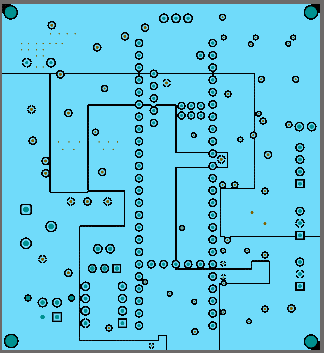
Multiple Voltage Power Plane
All polygon pours on signal layers (Layers 1 and 4) should default to GND, unless there's a specific reason to pour another net. In those cases, keep the pour away from sensitive routing and ensure it's well stitched with vias to the internal ground plane. Use thermal reliefs (spoke connections) for pads and vias to balance manufacturability with electrical performance.
Finally, make sure to stitch GND vias liberally between the outer layers and the internal ground plane — especially near signal vias, layer transitions, and around the board perimeter. This minimizes impedance discontinuities and forms a solid return path network.
Polygon Pour Keep-Out Areas
There are cases where you do not want a polygon pour to fill a region. Common examples include:
In Altium, you can define keep-out areas specifically for polygon pours. Simply draw the region inside your pour, and it will be excluded. This works per-polygon, so if you have multiple pours over the same net, each one needs its own cutout.
Teardrop Connection
Sometimes increasing trace width to better connect to a via or pad is not possible.
If this is the case, a teardrop connection can be used. A teardrop connection keeps the trace width the same, but gradually widens it as it connects to a via or pad. This helps with all of the issues outlined in the previous section, but also allows for connection of impedance matched traces. This gradual transition between the impedance matched width and the pin/via/pad reduces the impedance discontinuity.
For differential signals, it is suggested to refrain from using this type of connection, as it may cause issues due to the space between traces changing.
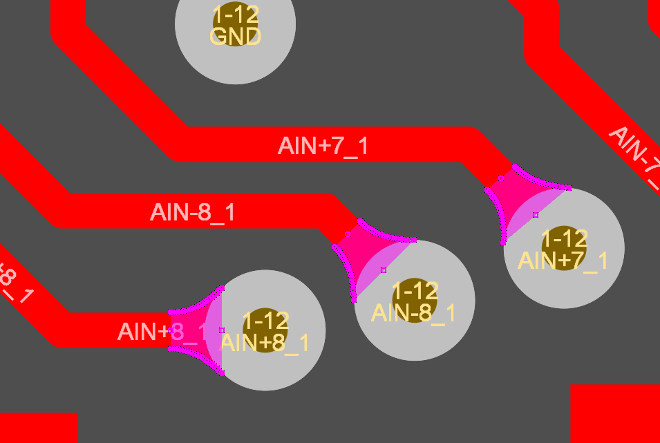
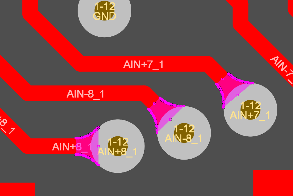
Teardrop Connection Type
Signal Return Paths
A clean and low-impedance return path is crucial for signal integrity and EMI reduction. On a multilayer PCB, return currents typically flow in the nearest reference plane directly underneath the signal trace.

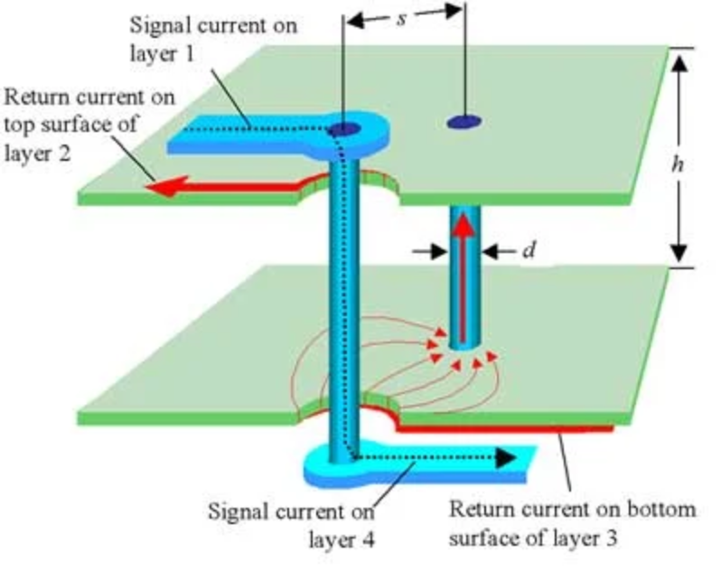
Return Path Visualization
For high-speed or sensitive signals, ensure that the signal trace runs over a continuous solid ground plane without gaps or splits. Interruptions in the ground plane force return currents to detour around voids, increasing loop area and causing unwanted noise and radiation.
When signals transition between layers through vias, provide nearby ground vias to maintain a continuous return path and minimize loop inductance. Multiple ground vias around high-speed signal vias help reduce impedance discontinuities.
Avoid routing signals over isolated copper islands or split planes, as these can break return current paths and degrade signal quality.
By maintaining well-planned return paths, you reduce crosstalk, improve EMC performance, and enhance overall board reliability.
Impedance Matching
Impedance matching ensures that a signal trace's impedance closely matches that of the source and load, which is typically 50 50 Ω for single-ended and 100 100 Ω for differential pairs. This becomes critical for high-speed signals (e.g., clocks, USB, SPI, and fast parallel buses), where mismatches can cause reflections, degraded signal integrity, or outright communication failures.
In a 4-layer stackup like SIG/GND/PWR/SIG, maintain controlled impedance by routing high-speed signals on the outer layers directly over the adjacent ground plane. The trace width, the dielectric thickness between layers, and the trace's distance to its reference plane all affect the impedance. Routing over power planes should be avoided for impedance-sensitive signals unless the power plane is well-decoupled and quiet—use ground as the primary reference.
You can calculate trace dimensions for controlled impedance using Altium's Layer Stack Manager and Impedance Profile tools. For an external check or second opinion, Saturn PCB Design Toolkit is widely used to perform quick impedance and stackup calculations. While it doesn't replace a professional fabricator’s tools, it's often close enough for practical design decisions. Ask for help from alumni or older members to verify calculations.
Focus impedance control efforts on critical nets, as not every signal needs matching.
Differential Pairs
When routing:
Via Stitching and Shielding
Via stitching involves placing multiple vias to connect copper pours (usually ground) between layers, improving return paths, shielding, and EMI performance. In a 4-layer board, stitching your ground pours together across layers (e.g., Layer 1 SIG to Layer 2 GND, or Layer 4 SIG to Layer 2 GND) ensures a low-impedance path for high-frequency return currents and minimizes loop area.
Use via stitching around high-speed traces and differential pairs. This helps shield signals from external noise and reduce radiation.
Stitch your power pours to the power plane with multiple vias near decoupling capacitors and ICs to reduce inductance and maintain low impedance across the power distribution network. This improves transient response and helps suppress power plane noise.
Careful via stitching strengthens the physical and electrical integrity of your multilayer design.
Unique Situations
Here are some unique situations that did not have a section:
Design Validation
Trace Validation
Polygon Pour Validation
Ground and Power Plane Validation
Adding Your Name and Graphics
Make sure to add:
When you add these graphics, make sure it is on the Bottom Overlay or Top Overlay.Overlay. If you add it to one of the layers, it gets created out of copper, which is bad. If you decide to add something to the Bottom Overlay,Overlay, you will have to mirror the image for it to print correctly.
Generating PCB Outputs
Output Job File
Verifying Gerber and Drill Files on JLCPCB
Reference Material
General Reading Material
Altium Designer: PCB Design Documentation
Youtube
Saturn PCB Toolkit
Document Revision Notes
06/07/2025: Created the document, created and updated sections with starting info (B. White, Rev 0.1)
07/23/2025: Reformatted document to include two-layer board design as well (B. White, Rev 0.5)
08/01/2025: Migrated guide to new SCR wiki (B. White, Rev 0.5)
10/08/2025: Migrated guide to new SCR wiki (B. White, Rev 0.5)