
Altium: Producing PCB artifacts for JLCPCB
Producing the artifacts
Guide for how to create PCB artifacts for ordering PCBs through Altium for JLCPCB.JLCPCB
1. Run the DRC (Design Rule Checker)
In Altium, go to Tools > Design Rule Check... In the pop-up window, click Run Design Rule Check....
Verify that there are no important issues. For example, you can ignore violations regarding "Silk" (silk screen) and some clearance violations. This comes with practice to know which violations are or aren't important.
Advanced You can customize your DRC to use rules that are specifically tuned for JLCPCB. Download the
RUL(rules) file at the JLCPCB link in Step 2. See https://www.altium.com/documentation/altium-designer/defining-scoping-managing-pcb-design-rules#!exporting-and-importing-rules for instructions on how to import rules.This is not necessary for verifying most important problems. {.is-info}
2. Create the artifacts
Follow the instructions for Generating Gerber file and Generating NC Drill File at https://jlcpcb.com/help/article/8-How-to-export-Altium-PCB-to-gerber-files
3. Zip the artifacts
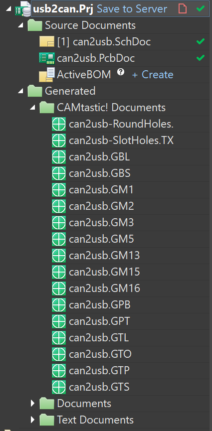
Once you have completed the steps above, you should see several new files under your Altium project, as seen below. Your files may differ depending on your project, but there should be some.
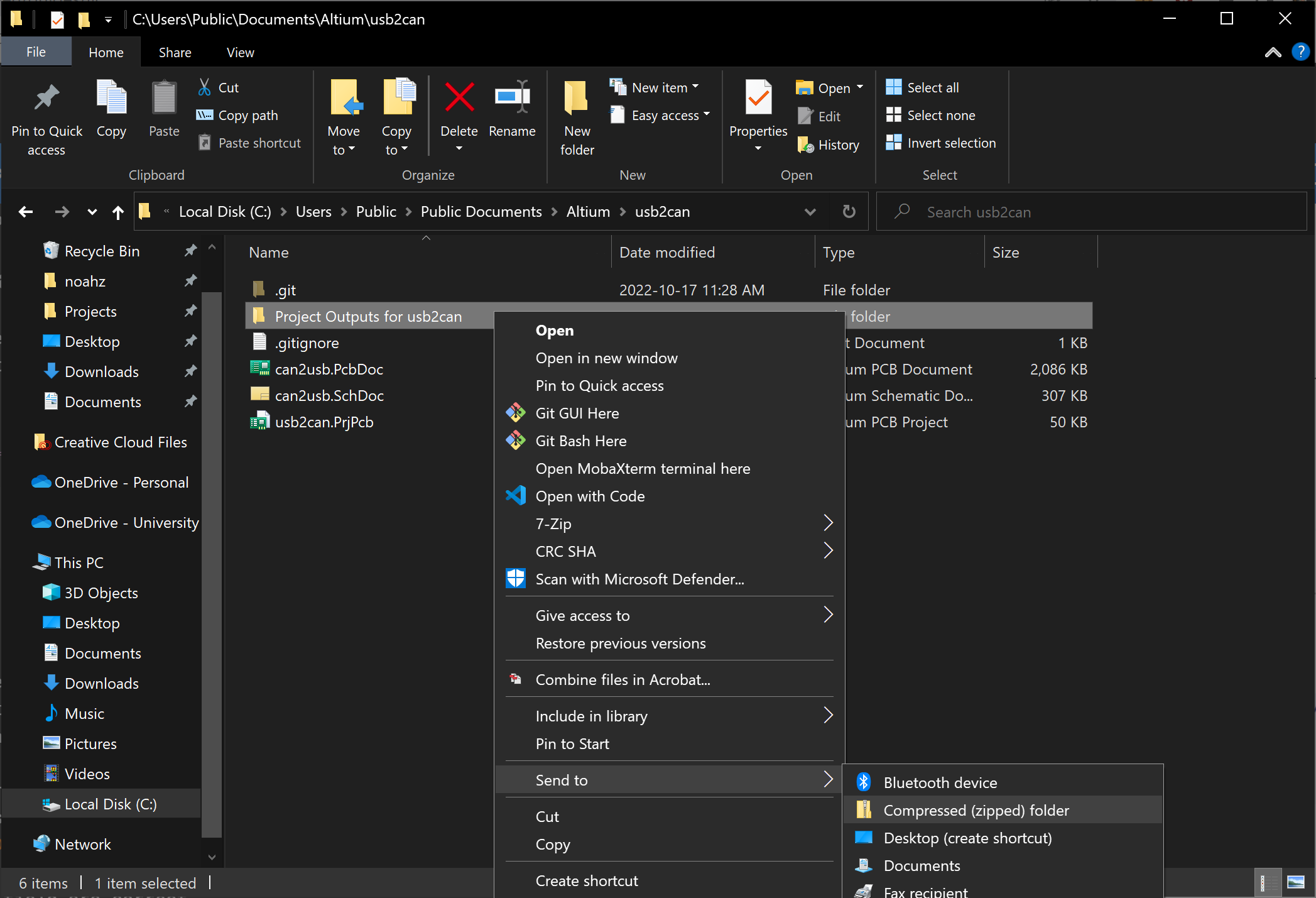
Finally, we need to zip all the files. Right click any of the files and select Explore. This should open the folder all your files are contained inside. Navigate to the parent folder. Then, right click the folder with all your artifacts and zip it up, as seen below.
Congrats! You now have a zip file ready to be uploaded to JLCPCB and be ordered.
Verifying the artifacts are correct
Verify your zip file will work by uploading it to the JLCPCB ordering page at https://cart.jlcpcb.com/quote (This is just to verify, you aren't actually going to order anything!)
Once you upload your zip file, JLCPCB will take a few seconds to process. After it is done, it should look like the screenshot below. Make sure it says Detected X layer board of YxZ at the top and that the values are correct. Also make sure the autopopulated values in the Dimensions field are correct.
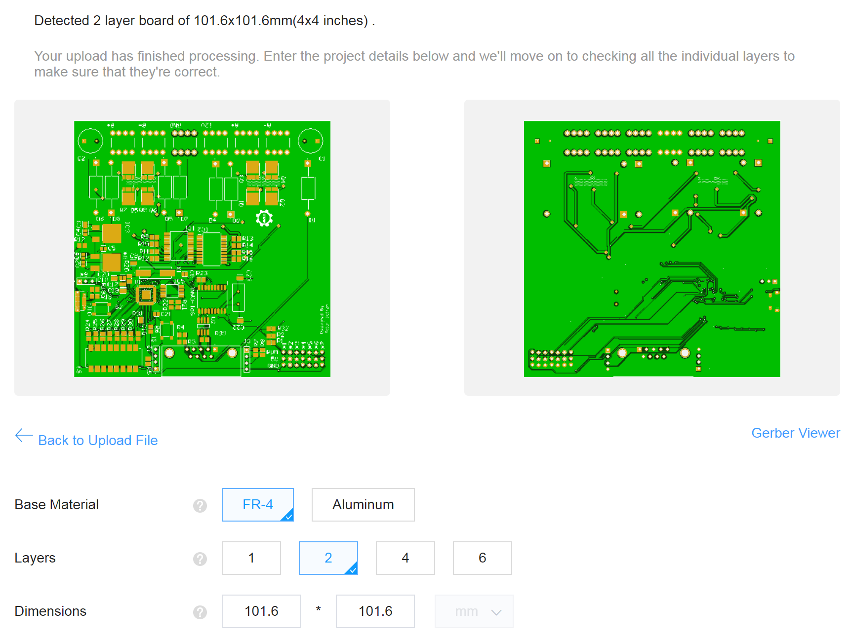
Finally, click on the Gerber Viewer link below the PCB preview images. Here you can view exactly how the PCBs will be manufactured. Make sure the top and bottom layers look correct, your silk screen is correct, and the drill holes are actually holes.