
1. Project Creation (WIP)
Introduction
This page includes a quick overview about how to use the PCB Design Software - Altium. You'll learn the basic process on how Printed Circuit Boards (PCBs) are made by using the tools in Altium.
For additional information on learning the Altium basics, please access the tutorial page on their website: Altium Tutorials
Goals
-
Learning
- How are Printed Circuit Board Made?
-
What is Altium and how do you use it?
-
Practical
-
Creating a circuit schematic
-
Developing a board layout and conducting a Design Rule Check
-
Preparing a board design for manufacturing
-
This tutorial is a Work in Progress!
Before starting your project, make sure you created are added to the Sooner Competitive Robotics Altium Workspace and have an account created.
PCB Basics
InformationA on:
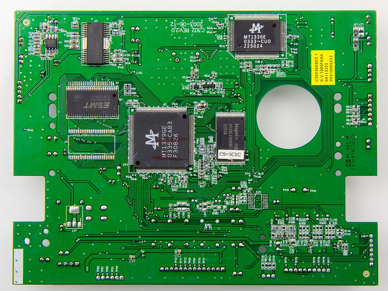
https://en.wikipedia.org/wiki/Printed_circuit_board
For more information on how PCB works, check out this video: What are PCBs? || How do PCBs Work?
Altium Designer

Altium is the premier industry-level PCB design software. Engineers primarily use Altium
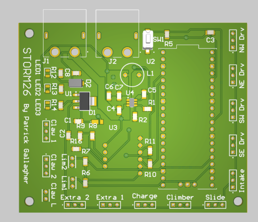
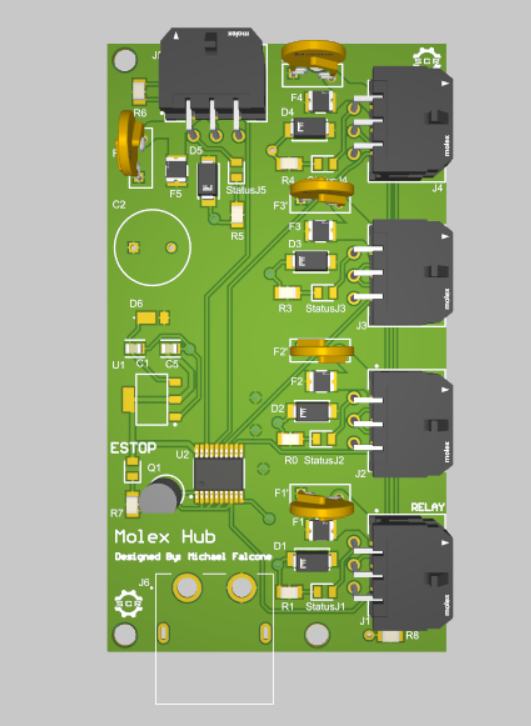
because it has a working unified design system, allowing you develop schematics, layouts, component libraries, manufacturing drawings, PCB CAD models, and much more in a single software.This makes Altium the ideal software for our robotics team. Below are examples of PCBs developed for our robots over the years:
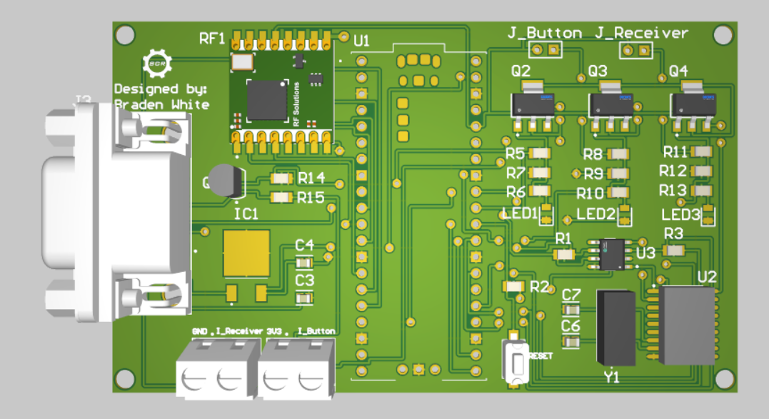
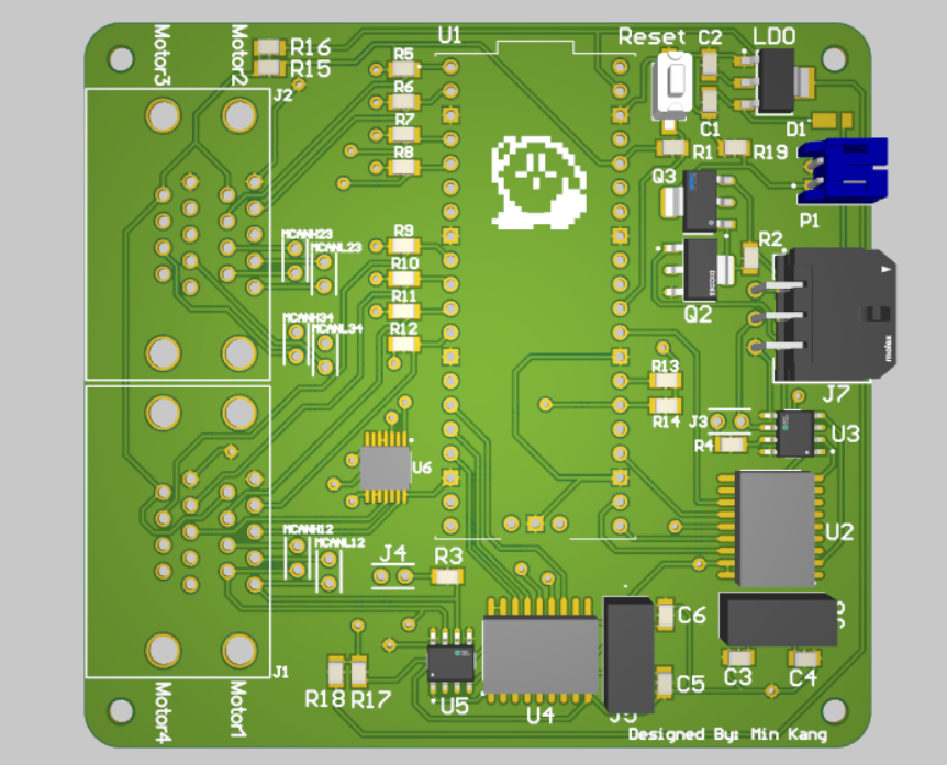
Project Overview - SPI-CAN Breakout Board
InsertFor Informationthis Here.Altium tutorial, your goal is to recreate the PCB found below, the SPI-CAN Breakout Board..
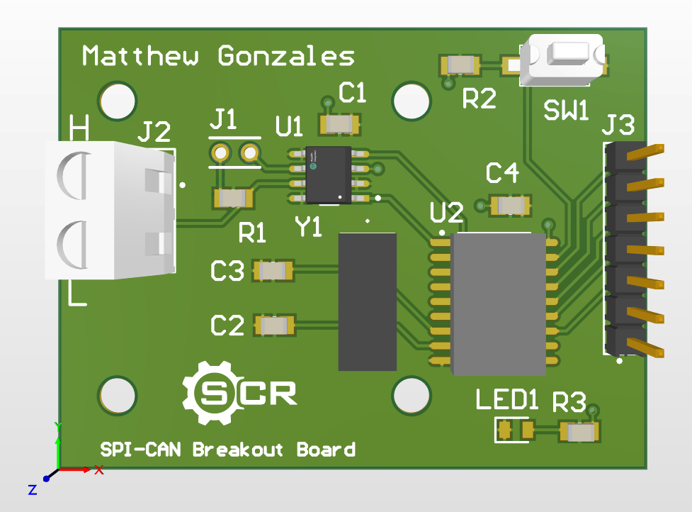
The SPI-CAN Breakout board
This board is a revision of the the CAN-SPI Breakout Board from the 2026 IGVC Team, designed by Luke Finnegan.
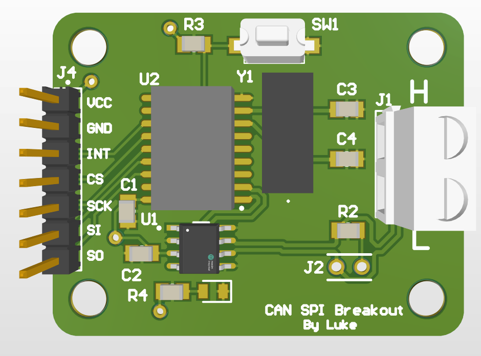
Creating a Project
To start, open the Altium application on your device. Upon Altium loading, you should be greeted by a home page that looks similar to below:
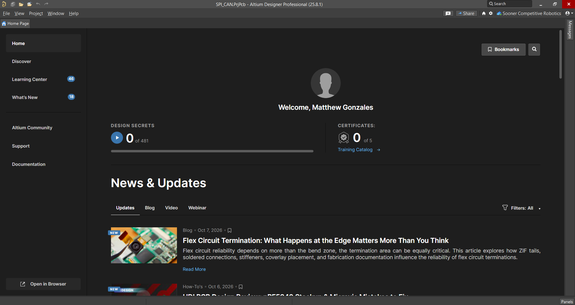
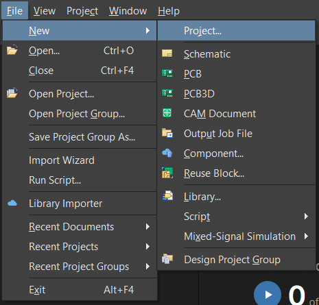
To start a new project, navigate to the top-left toolbar and select File --> select select New --> then select select Project
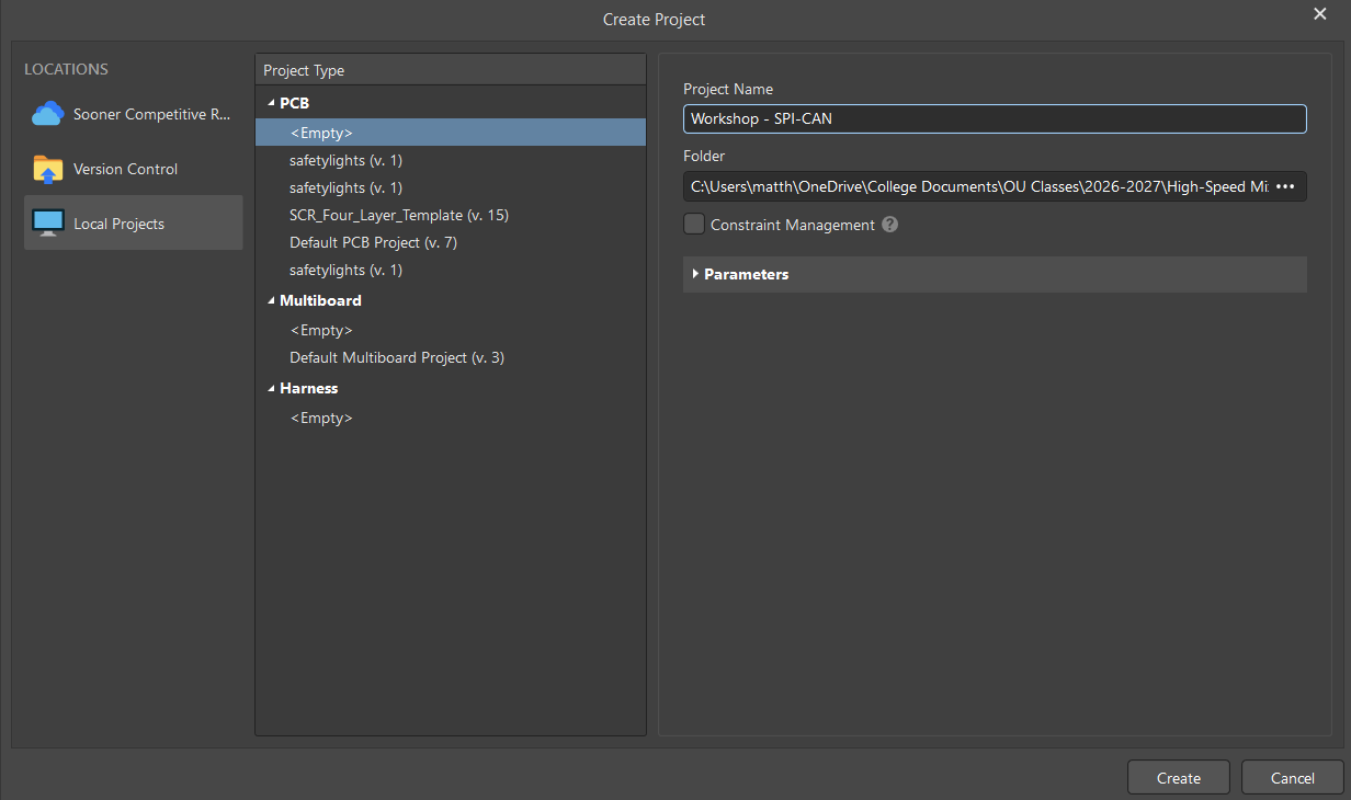
In the new window under Project Name, name your project "Worshop - SPI-CAN"
- Under Folder, make sure your project is saved in a file location you can find. You can change the file location by selecting the three dots "..." on the right.
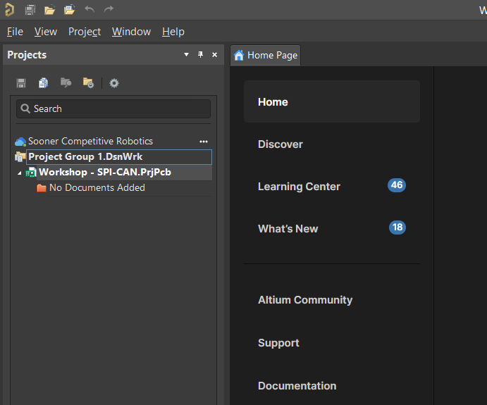
Upon creating a new project, the Projects Panel will now open, where you can view all projects you have open.
- In addition, your project's repository will be saved in the Sooner Competitive Robotics workspace.
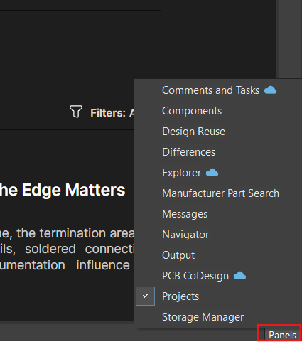
On the bottom right of your window, you'll find the Panels toggle. This toggle stores a ton of tools and will come in handy later. For now, just know you can reopen the Projects panel through accessing this toggle.
Adding to a Project
Now, your project is currently empty. To get started, you'll need to add documents by right-clicking on the "Workshop - SPI-CAN.PrjPcb" icon. In the new window, hover over Add New to Project, then you can add any documents you need.
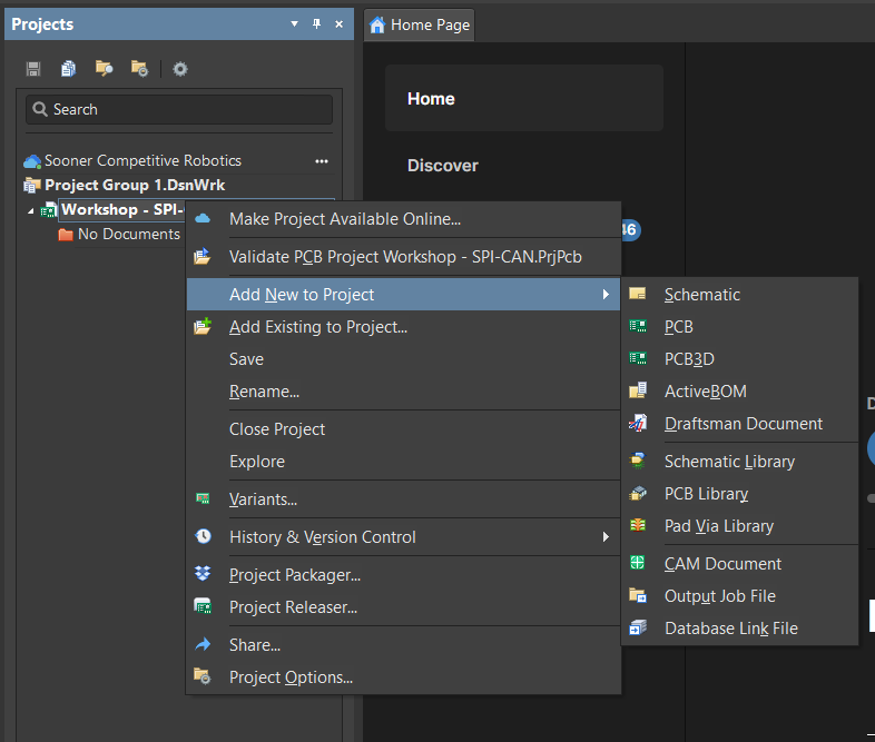
Go ahead and add the following documents to your project:
- Schematic
- PCB
- ActiveBOM
- Draftsman Document
- Assembly Drawing
- Fabrication Drawing
- Output Job File
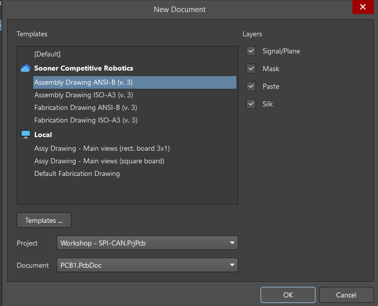
For the Draftsman Documents, a new window will appear. For the Assembly Drawing, select select Assembly Drawing ANSI-B (v. 3), then press OK. For the Fabrication Drawing, select select Fabrication Drawing ANSI-B (v. 3), then press OK.
After you add the required documents to your project, your Projects panel should look like the screenshot below:
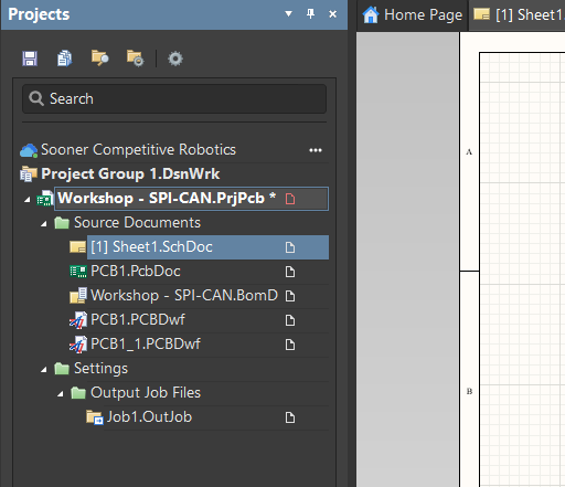
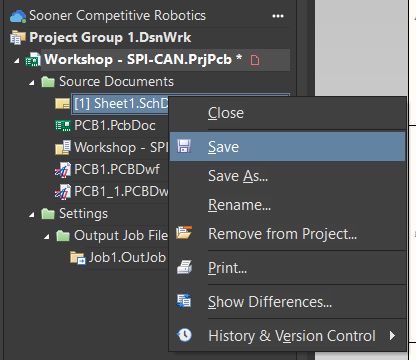
Before you start your design, you'll need to save each of your documents and rename them accordingly. To save a document, right-click on the document's icon, then select Save
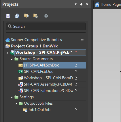
Rename each of the documents until they match the names below:
Congratulations! You just finished creating your first Project! Now, you can get started on the schematic by accessing the tutorial: 2. Creating a Schematic